Cynovex
1 / 5
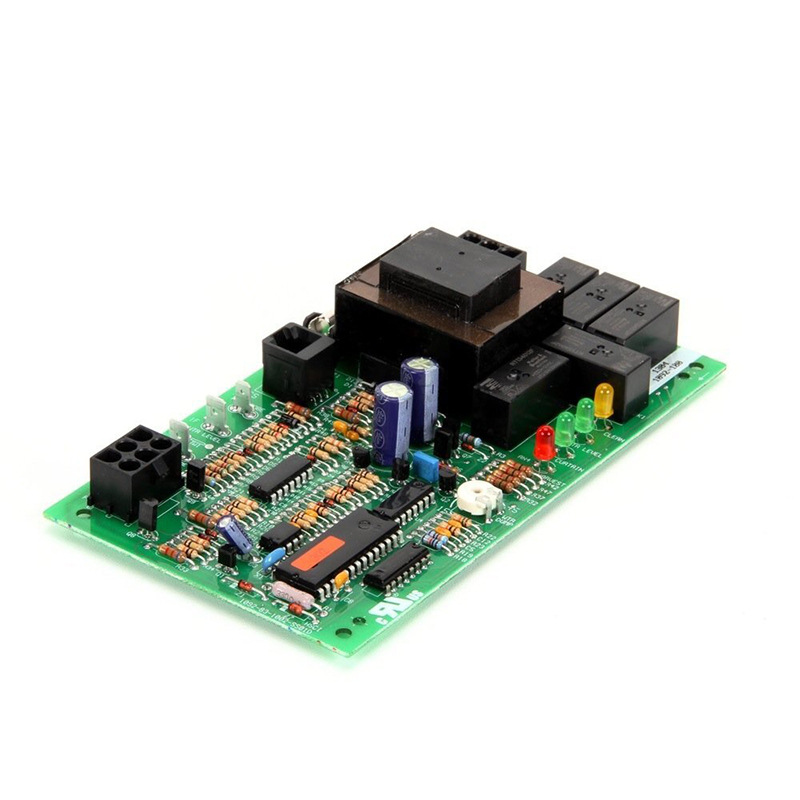
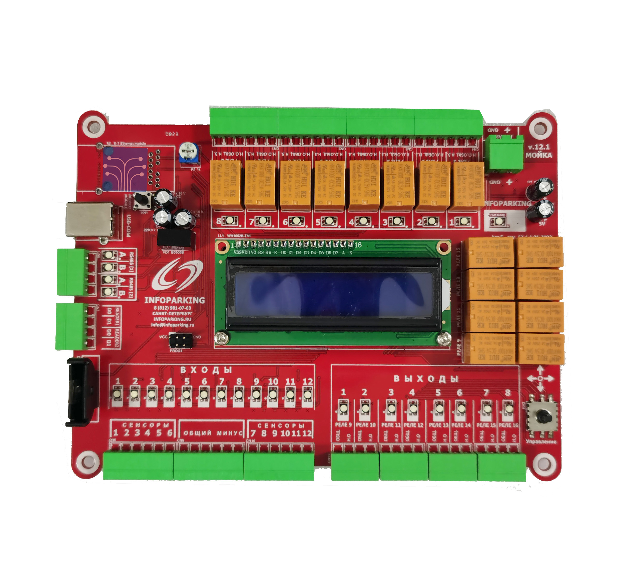
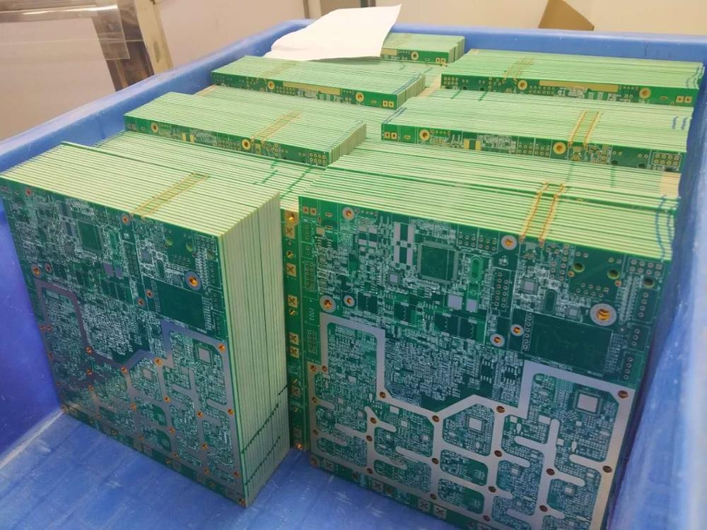
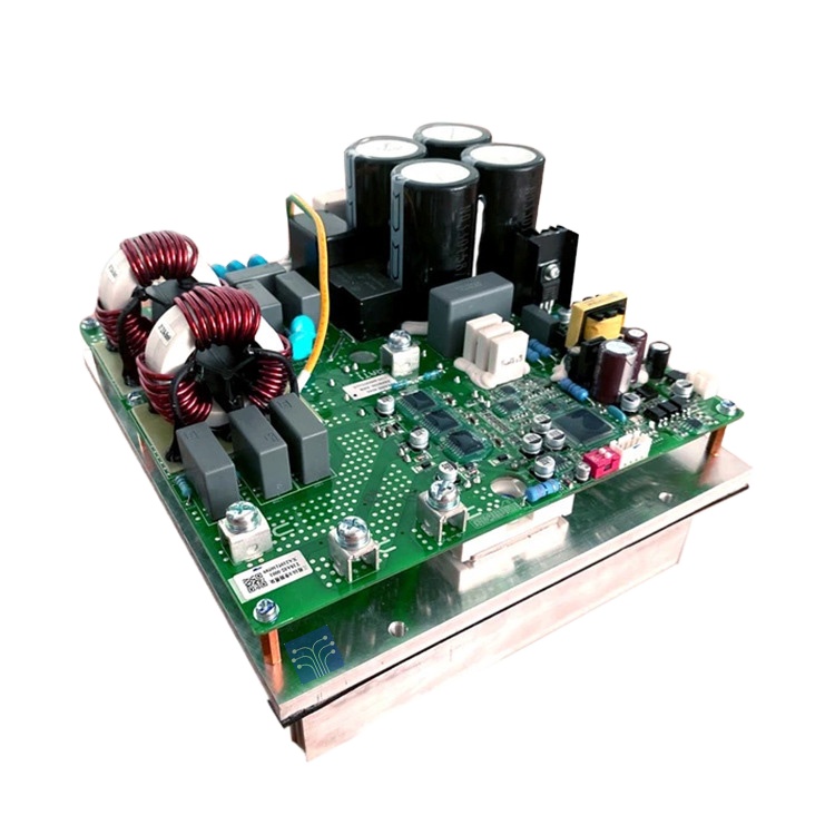
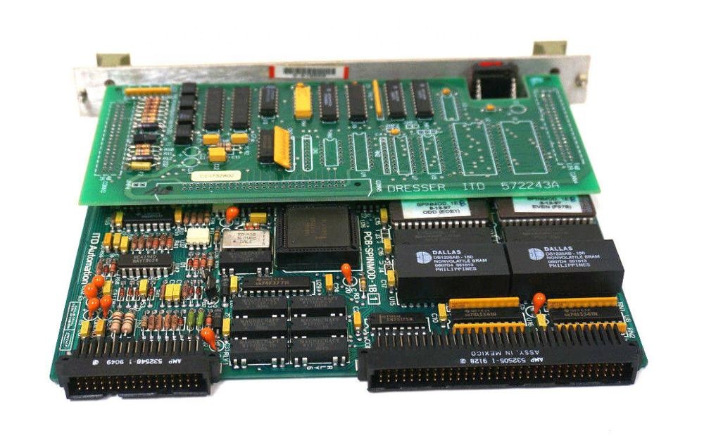
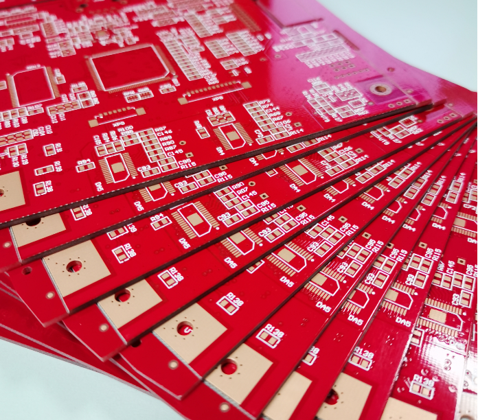
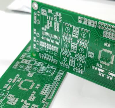
As PCBs are custom products, returns are not supported. For quality issues, please contact customer service for a refund or replacement. We do not bear any losses beyond the product value. Force majeure delays (power/water supply) will not be compensated.
Please communicate special instructions directly with customer service. Confirm process, quantity, and layers before payment. We are not responsible for issues caused by lack of technical understanding by purchasing personnel; please consult your engineer.
Orders placed before 17:00 are considered same-day. "24-hour delivery" refers to one business day. Delivery times exclude Sundays and holidays.
Standard: Green solder mask, white silkscreen, 1.6mm thickness, HASL, 1oz copper, vias with solder mask, line width/spacing 0.2mm, vias above 0.3mm. Gerber format required. Special processes require a new quotation.
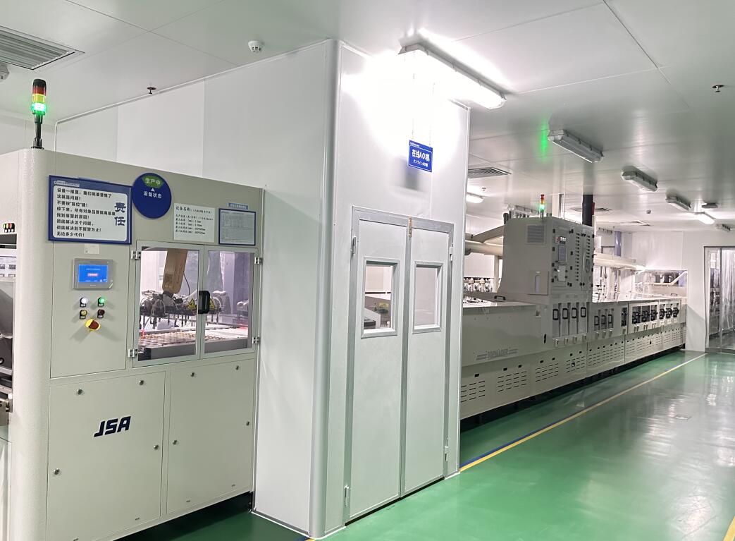
| Category | Volume Production | Sample Processing |
|---|---|---|
| Layer Count | 1-68L | 64 Layer |
| Max Thickness | 10mm (394mil) | 14mm (551mil) |
| Min Line Width/Space (Inner) | 2.2mil / 2.2mil | 2.0mil / 2.0mil |
| Min Line Width/Space (Outer) | 2.5mil / 2.5mil | 2.2mil / 2.2mil |
| Max Copper Weight | 6oz | 30oz |
| Min Hole Size (Mechanical) | ≥0.15mm (6mil) | ≥0.1mm (4mil) |
| Min Hole Size (Laser) | 0.1mm (4mil) | 0.05mm (2mil) |
| Max Panel Size | 1250mm x 570mm | 1320mm x 600mm |
| Aspect Ratio | 25:1 | 35:1 |
Megtron6, Megtron4, Megtron7, TU872SLK, FR408HR, N4000-13 Series, MW4000, MW2000, TU933.
Ro3003, Ro3006, Ro4350B, Ro4360G2, Ro4835, CLTE, Genclad, RF35, FastRise27.
Blind & buried holes, Via in pad, Semi-plating holes, Counterbore, Step mounting holes, Mixed RF PCB, Busbar PCB.
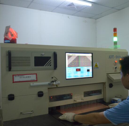
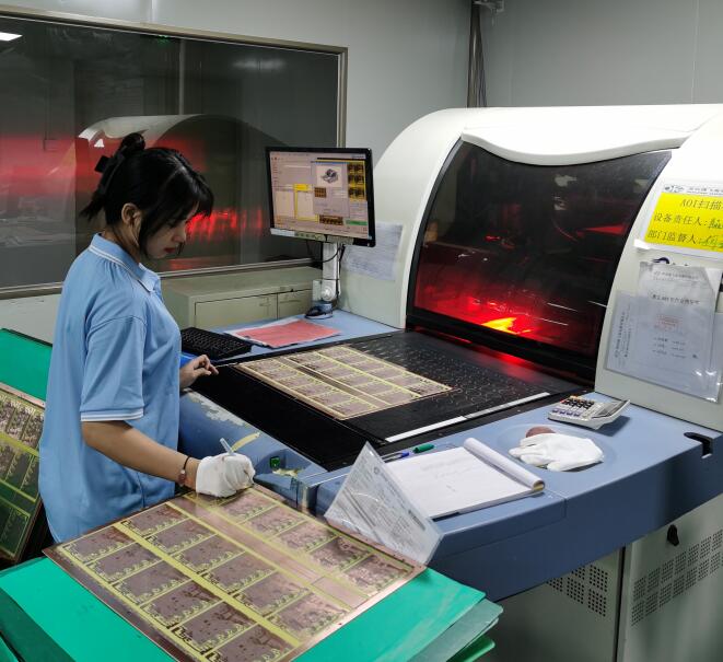

| Layers | Sample (Shortest) | Sample (Standard) | Mass Production |
|---|---|---|---|
| 2 layer | 24 h | 3 days | 6-7 days |
| 4 layer | 36 h | 5 days | 8-10 days |
| 6 layer | 48 h | 5 days | 8-12 days |
| 8 layer | 72 h | 5 days | 9-12 days |
| 10-14 layer | 4-5 days | 7-8 days | 14-16 days |
| 16-18 layer | 5-7 days | 9-10 days | 18 days |
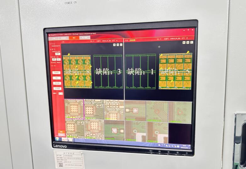
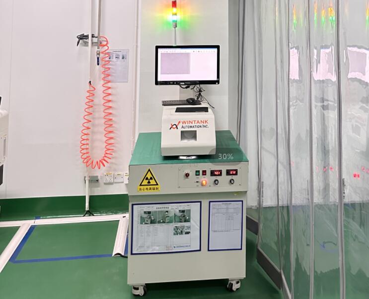
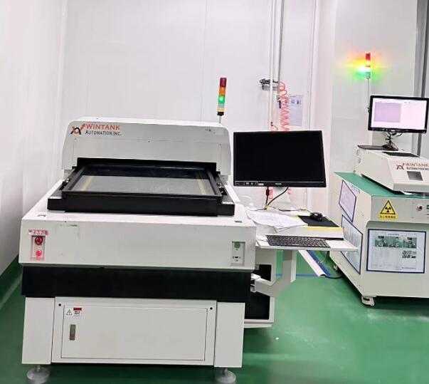
24h technical support & Gerber file handling. EQ completed within 4-8 hours. Support for 400+ new project reviews.
Formats: RS-274-X, RS-274-D, CAD, DXP, Protel 99 SE, PADS, GC-CAM.
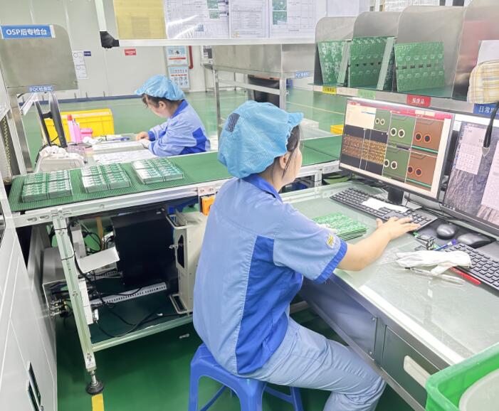
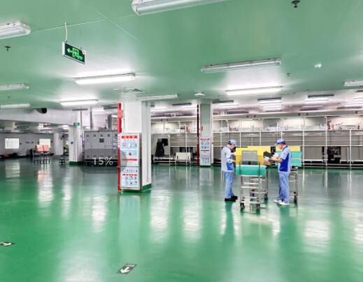
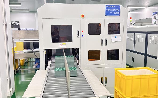
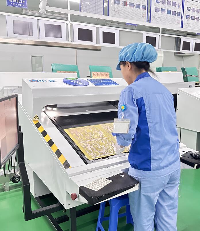
24-hour operations. Monthly production of 10K+ high-mix part numbers. 100+ QTA orders daily. One-step service from prototype to mass production.
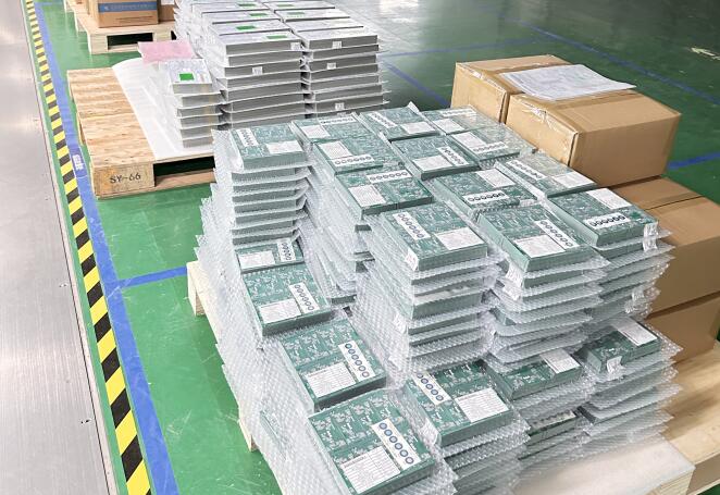
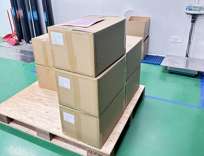
A: We can handle up to 68 layers for volume production and up to 64 layers for specialized sample processing.
A: We offer rapid prototyping with delivery as fast as 24 hours for 2-layer boards and 36-48 hours for 4-6 layer boards.
A: We work with high-frequency and high-speed materials including Rogers (Ro4350B, Ro3003), Megtron (6, 7), Polyimide, and various high-TG copper foil boards.
A: Yes, we specialize in HDI, blind and buried vias, via-in-pad, rigid-flex boards, and heavy copper (up to 30oz) applications.
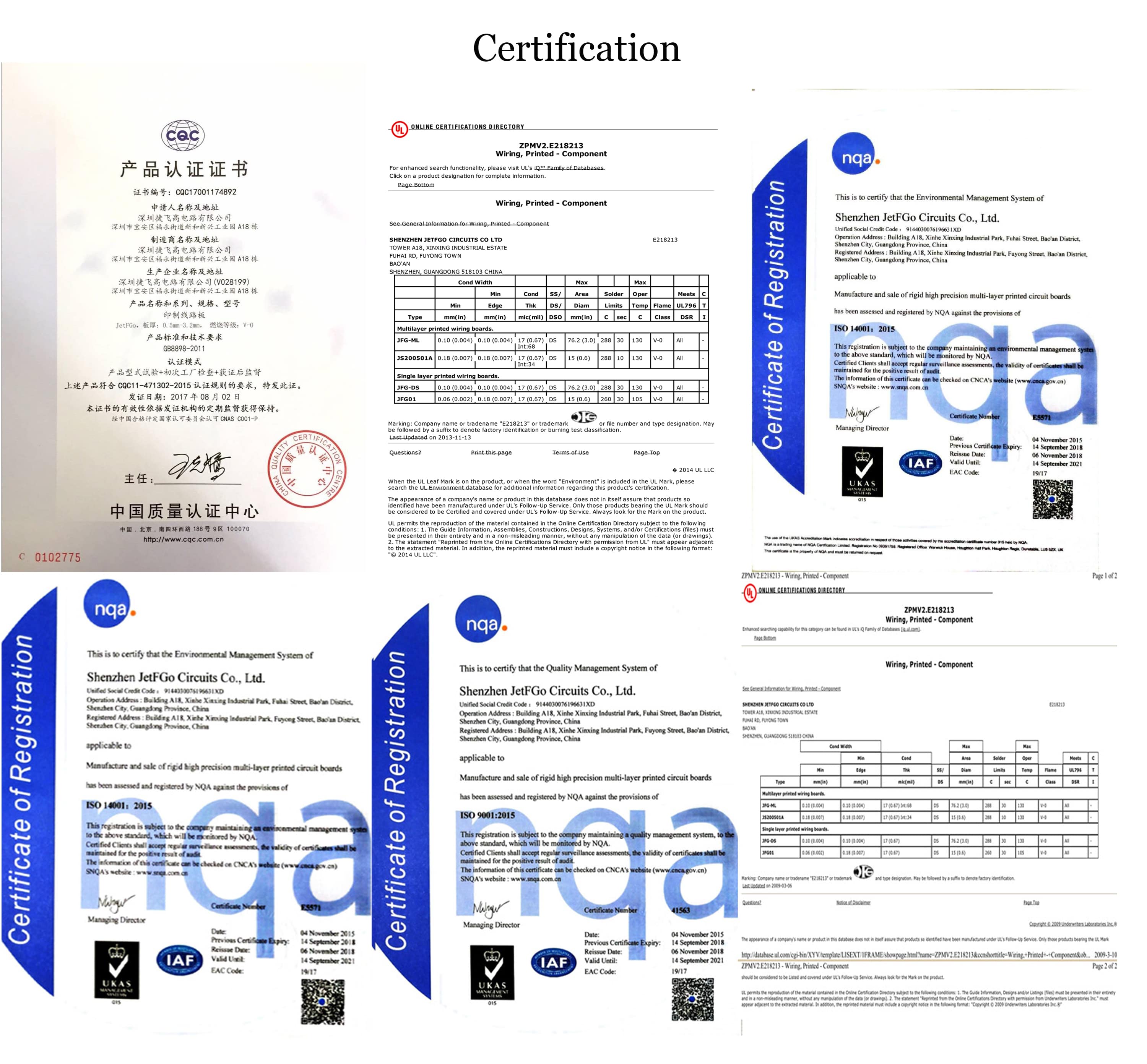
A: We strictly follow ISO 9001, ISO 14001, and IATF 16949 systems. All products are compliant with UL, CQC, RoHS, and REACH standards, ensuring 100% quality assurance.
A: We accept all major formats including Gerber (RS-274-X, RS-274-D), CAD, DXP, Protel 99 SE, PADS, and GC-CAM files.