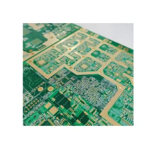
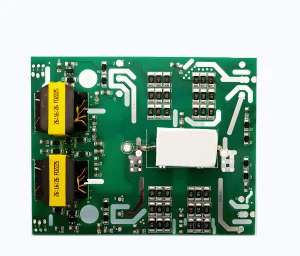
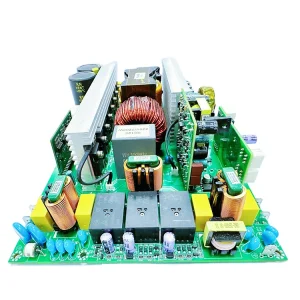
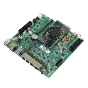
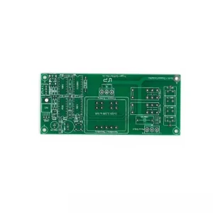
The electronics industry is undergoing a paradigm shift driven by AI, 5G, and IoT. As a leading PCB Multi-layer Circuit Board Manufacturer and Exporter, we recognize that the demand for high-density interconnects (HDI) has moved beyond consumer electronics into the realms of industrial automation, medical diagnostics, and aerospace telemetry. Modern multi-layer PCBs are no longer just conductive pathways; they are complex integrated systems that require sophisticated thermal management and signal integrity engineering.
Globally, the market is shifting toward "System-in-Package" (SiP) designs where the PCB serves as the substrate for multi-die assemblies. This requires manufacturers to possess not just etching capabilities, but also expertise in advanced laminates, blind and buried vias, and precision laser drilling.
Transitioning from 0.1mm to 0.05mm trace/space widths using mSAP technology to support 5G hardware.
Integration of heavy copper (up to 6oz) and ceramic substrates for EV power modules and high-wattage servers.
Utilizing Automated Optical Inspection (AOI) enhanced by machine learning to predict latent defects in inner layers.
Adoption of halogen-free materials and closed-loop water recycling systems in the PCB fabrication process.
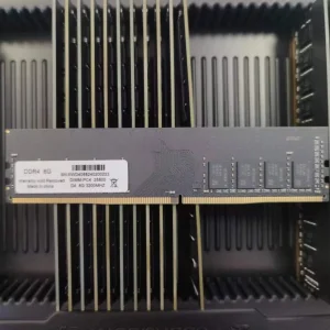
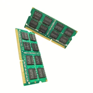
Founded in 2016, Cynovex Semiconductor Co., Ltd. has evolved into a powerhouse of high-performance DDR5 and multi-layer circuit solutions.
Integrating R&D, production, and quality control under one roof to ensure seamless global exports.
Trusted by over 1,150 supply chain partners across North America, Europe, and Southeast Asia.
Company Profile: Operating from a modern manufacturing facility covering 18,600 m², Cynovex integrates R&D, production, quality control, and international sales. Supported by an experienced engineering team and advanced manufacturing processes, we provide stable, high-speed memory and PCB products. Every product undergoes rigorous quality assurance using 100% functional testing, burn-in testing, compatibility testing, signal integrity testing, and aging tests. A dedicated team of 56 quality inspectors ensures that every shipment meets strict international quality standards.
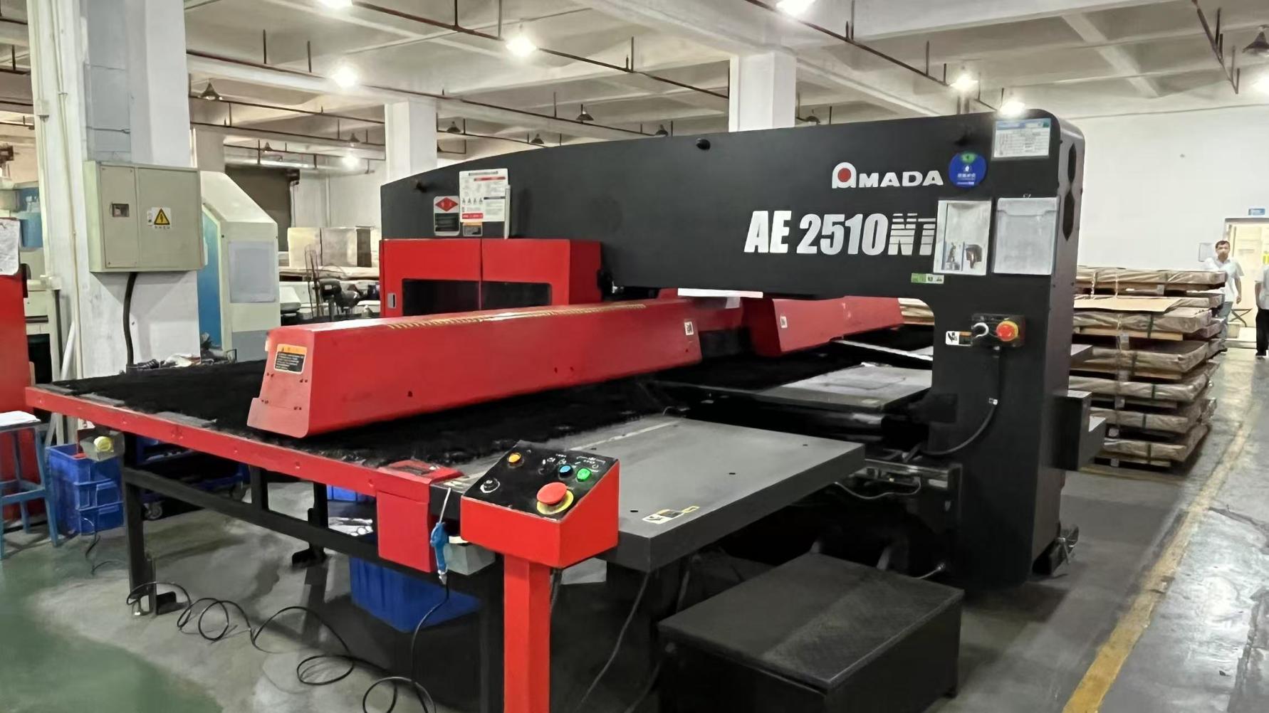
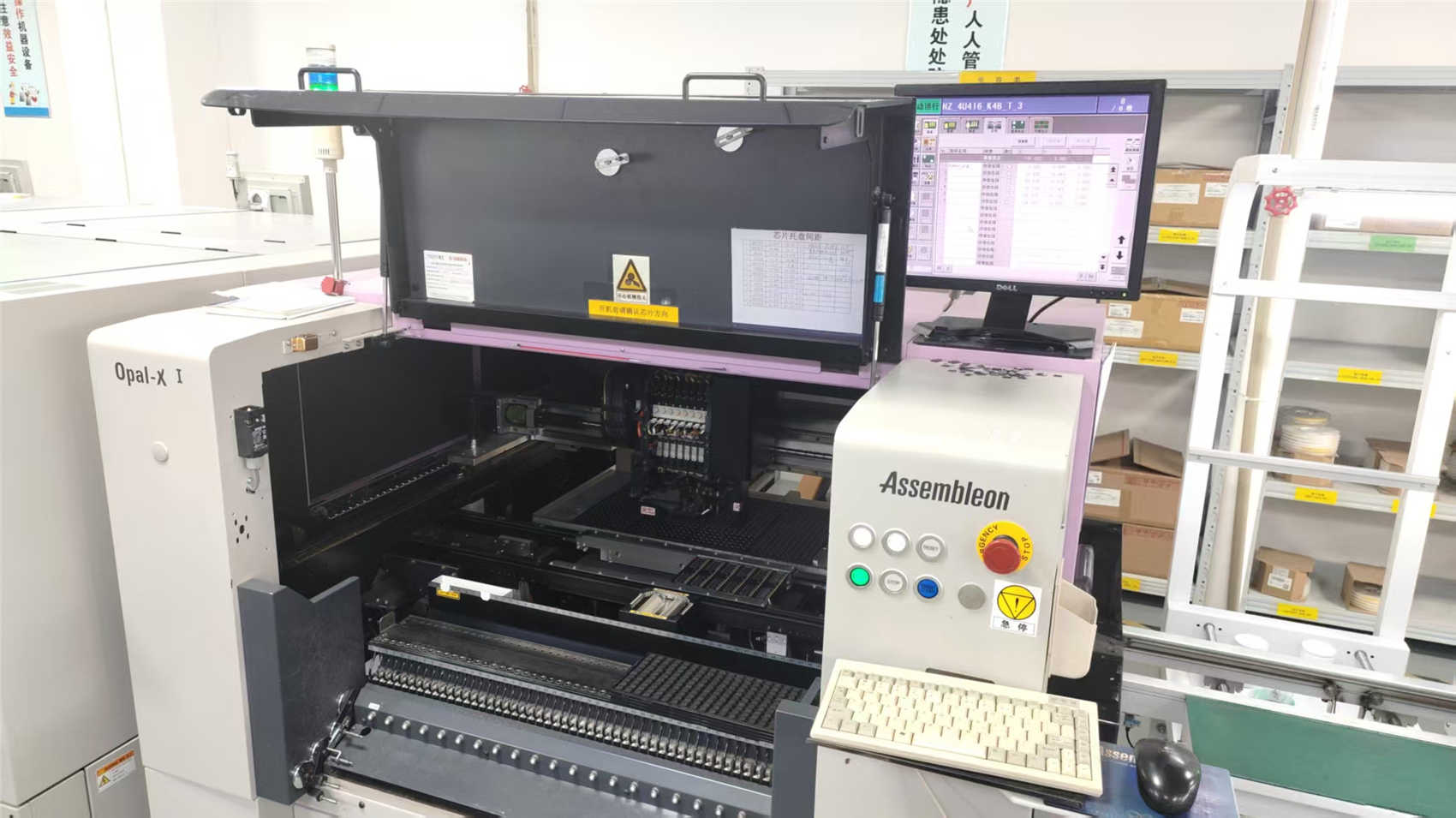
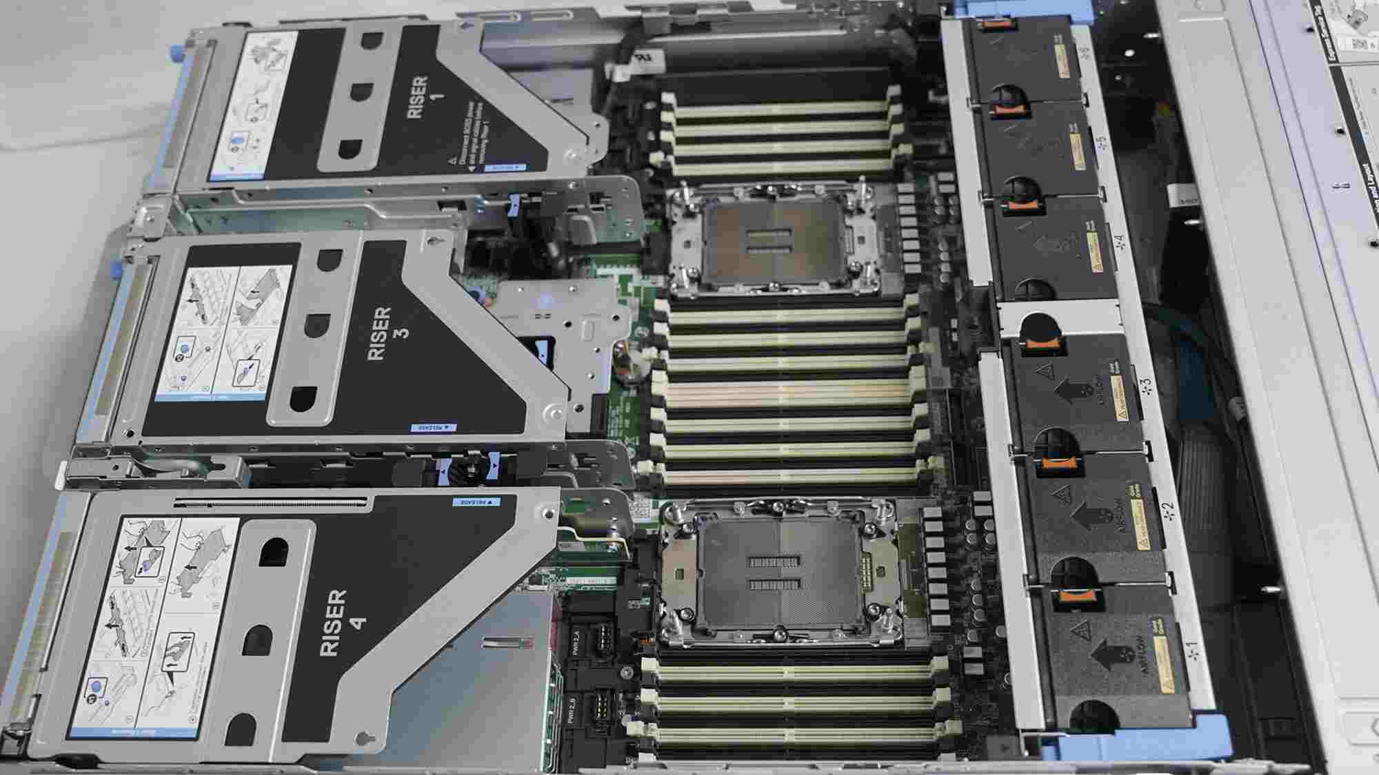
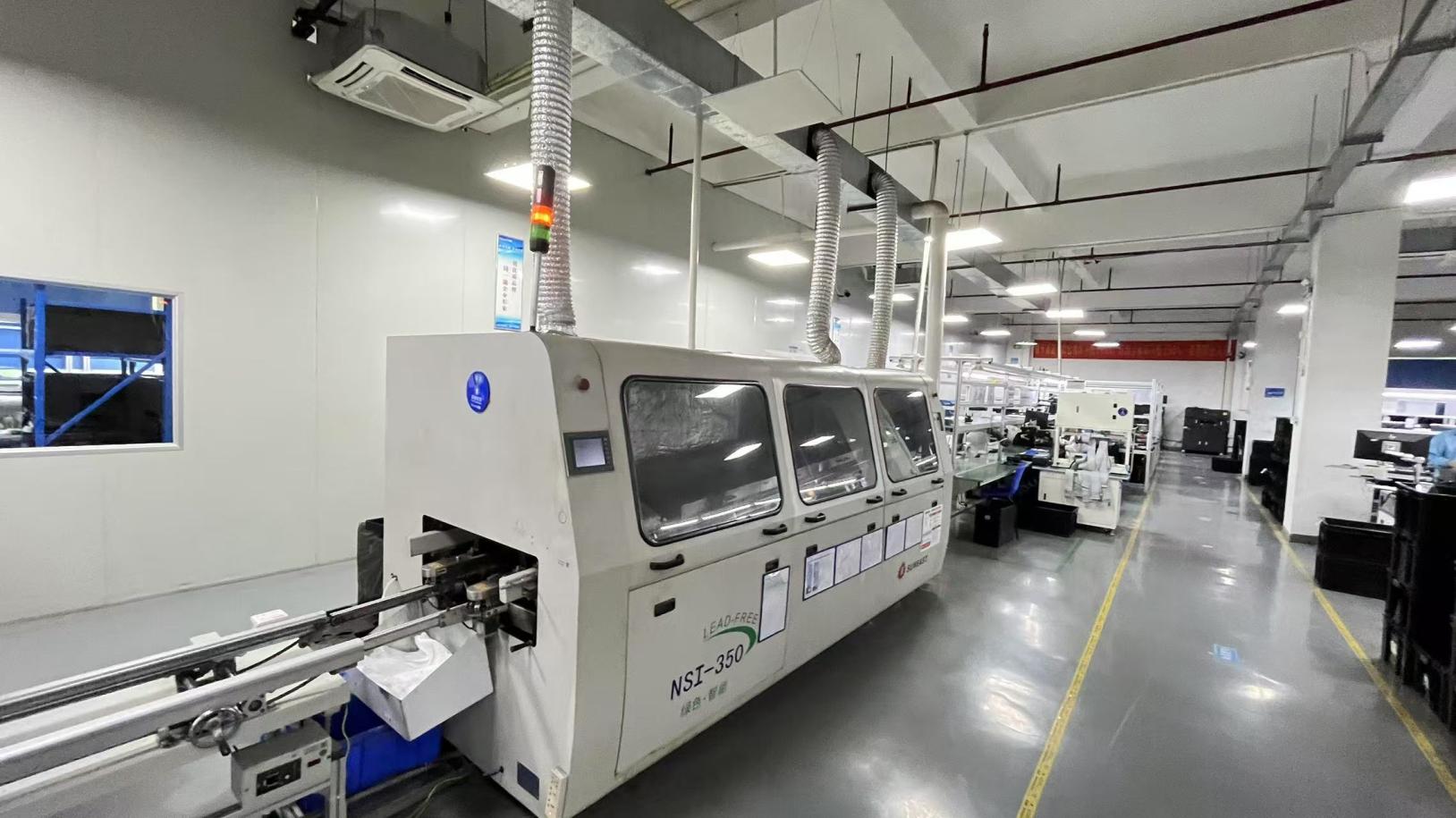
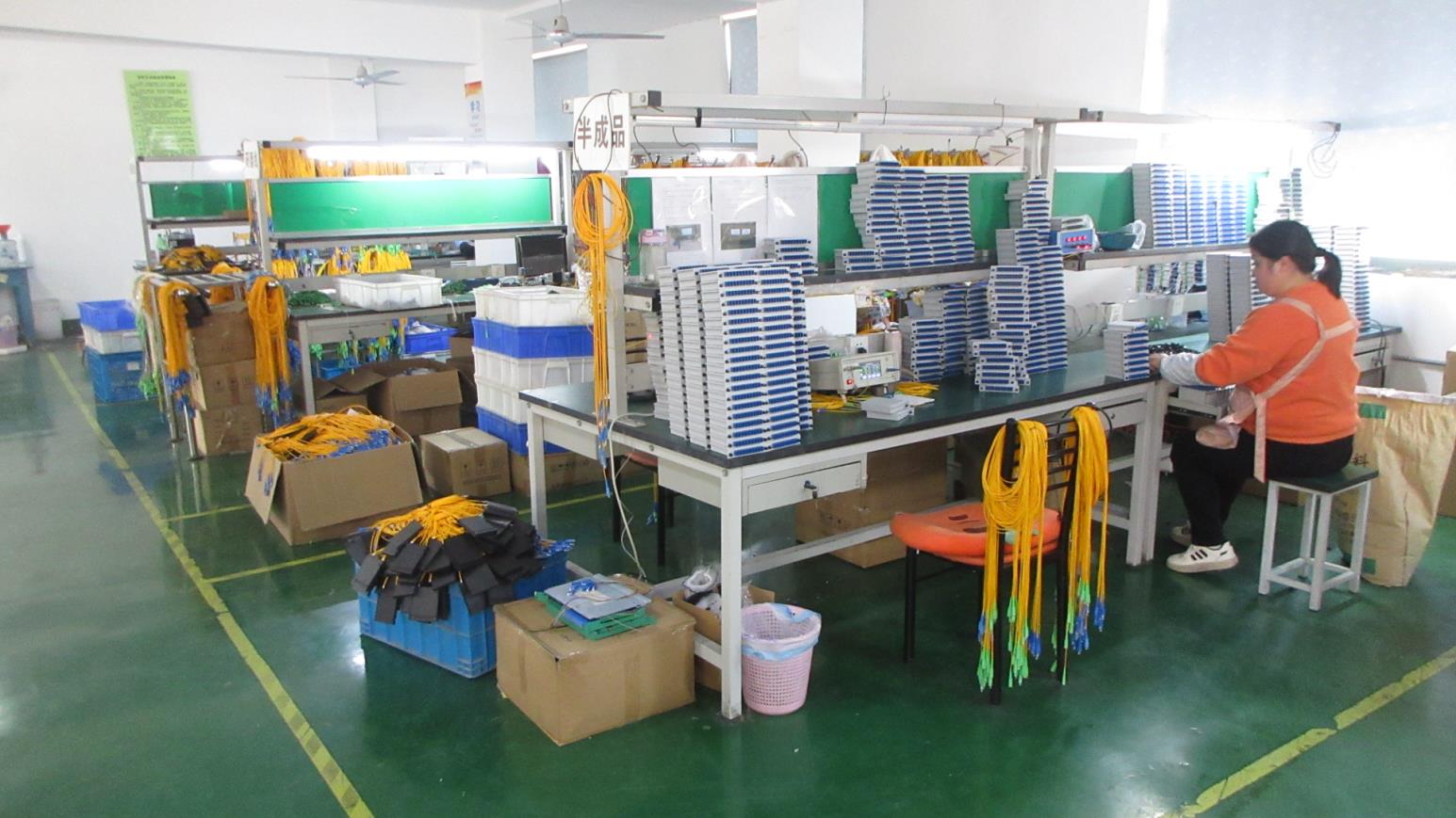
China remains the heart of the global PCB ecosystem, offering unparalleled supply chain resilience. The "China Advantage" is not merely about cost, but about the density of the ecosystem. Within a 50km radius of our facility, we have access to copper clad laminate (CCL) suppliers, chemical processors, specialized drill bit manufacturers, and high-speed logistics hubs.
We provide 24/7 technical support for our European and North American clients, ensuring that design modifications and DFM (Design for Manufacturability) reports are processed within a 12-hour window.
Our boards meet UL 94V-0, RoHS, and REACH requirements. We employ IPC-A-600 Class 2 and Class 3 standards depending on the mission-critical nature of the application.
 Cynovex