Cynovex
1 / 5
| Items | Capacity |
|---|---|
| Material | FR4, (High Tg, General Tg, Middle Tg), Lead-Free Solder Sheet, Halogen Free FR4, Ceramic Filling Material, Teflon, PI Material, BT Material, PPO, PPE etc. |
| Board thickness | Mass production: 394mil(10mm) Samples: 17.5mm |
| Surface finish | HASL, Immersion Gold, Immersion Tin, OSP, ENIG + OSP, Immersion Silver, ENEPIG, Gold Finger |
| PCB Max panel size | 1150mm × 560mm |
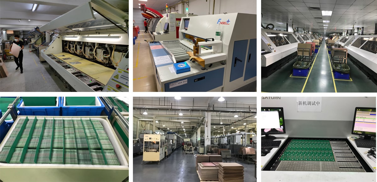
| Layer | Mass production: 2~58 layers / Pilot run: 64 layers, Flexible PCB: 1-12 Layers |
| Min hole size | Mechanical drill: 8mil(0.2mm) Laser drill: 3mil(0.075mm) |
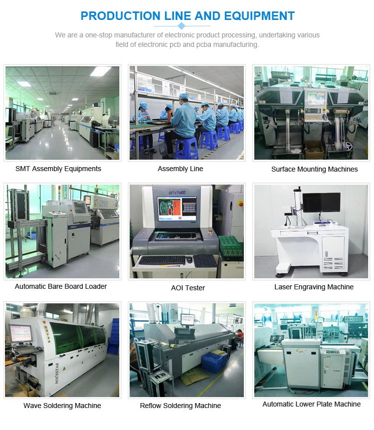
| PCBA QC | X-ray, AOI Test, Functional Test |
| Special Process | Buried Hole, Blind Hole, Embedded Resistance, Embedded Capacity, Hybrid, Partial hybrid, Partial high density, Back drilling, and Resistance control. |
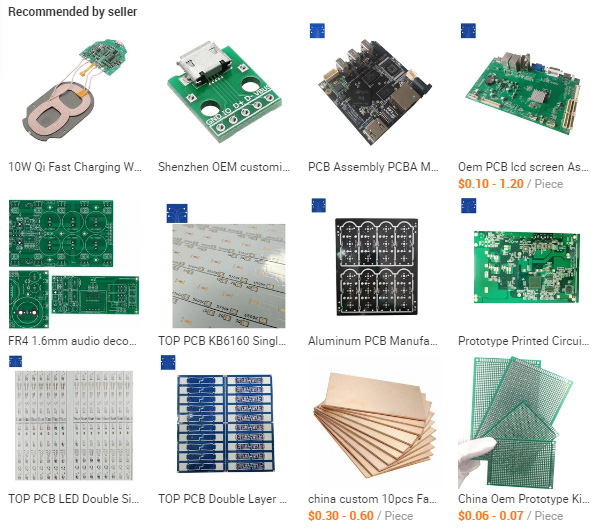
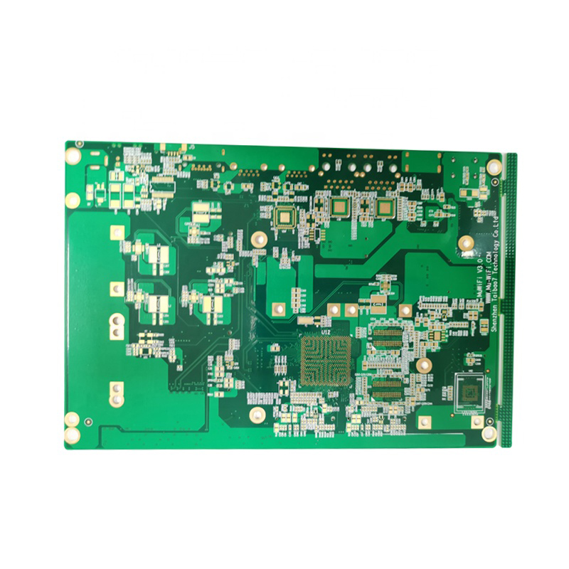
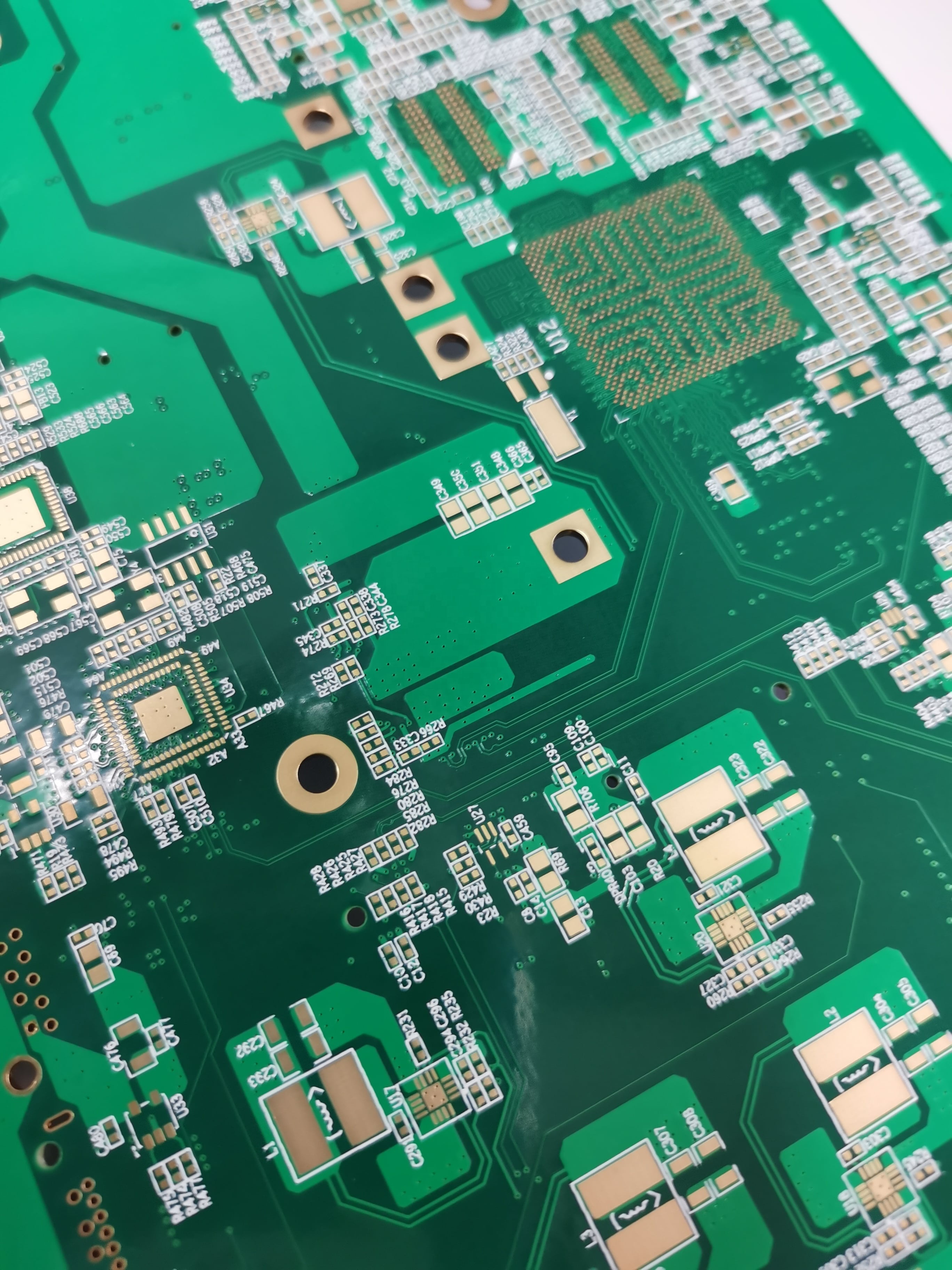
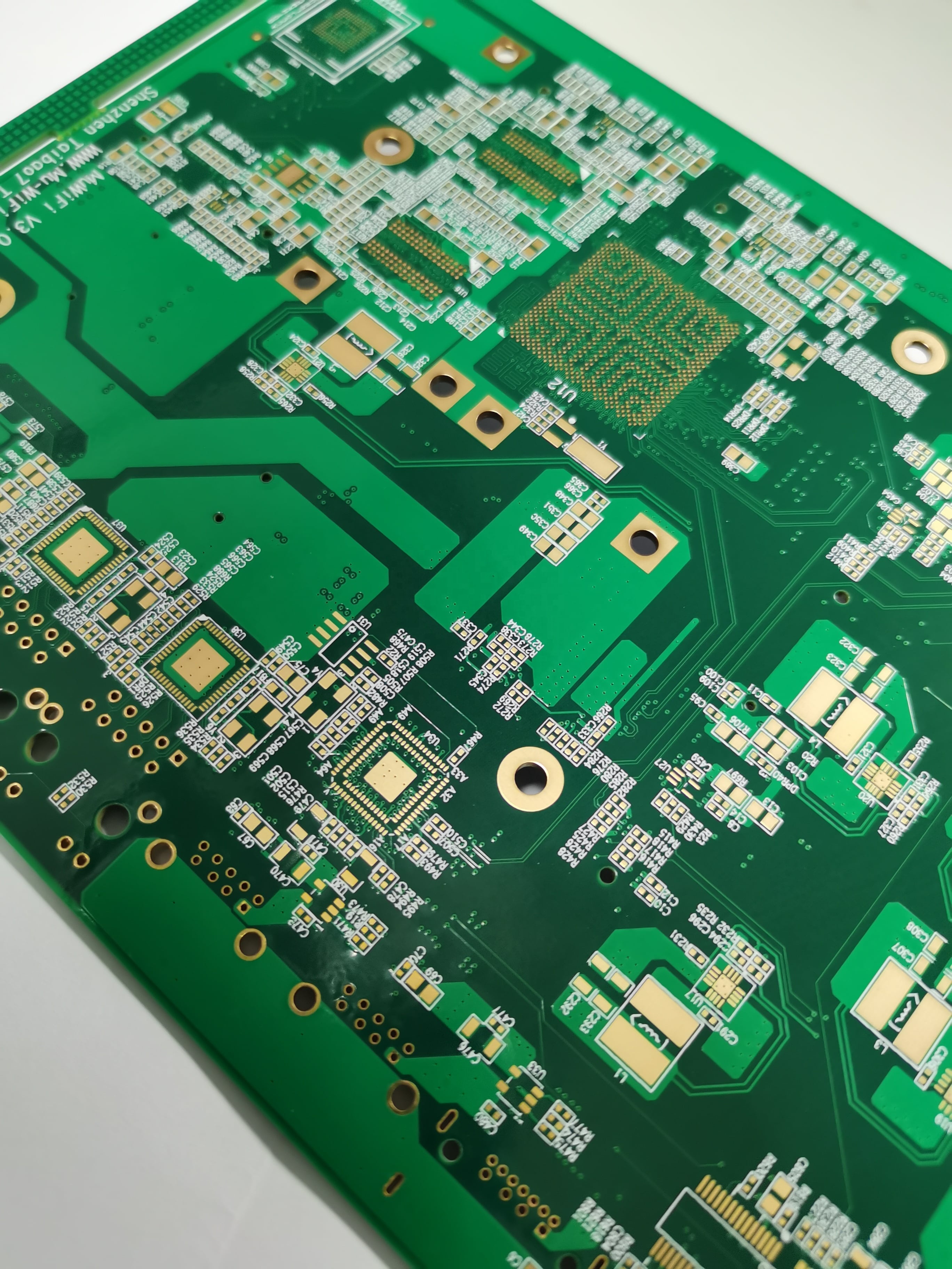
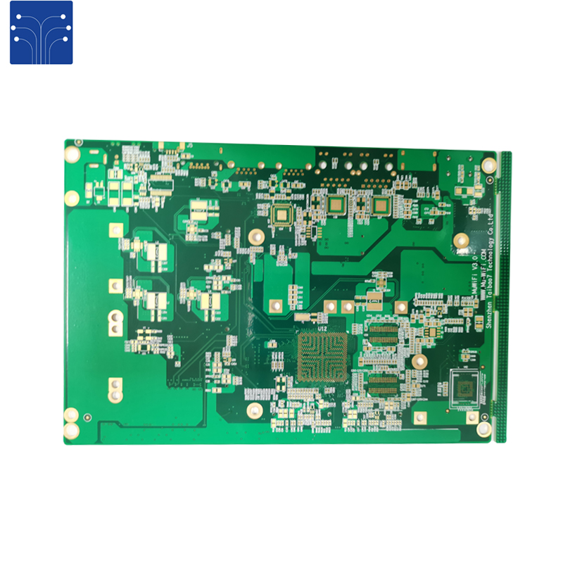
| Our service | PCB, Turnkey PCBA, PCB Clone, Housing, PCB Assembly, Component sourcing, PCB manufacturing from 1 to 64 layers, One stop services. |
| Sanforized | Buried via, Blind via, Mixed Pressure, Embedded Resistance, Embedded Capacitance, Local Mixed Pressure, Local High Density, Back drill, impedance control. |
| SMT Capacity | 700 Million Points/Day |
| DIP Capacity | 0.5 Million Points/Day |
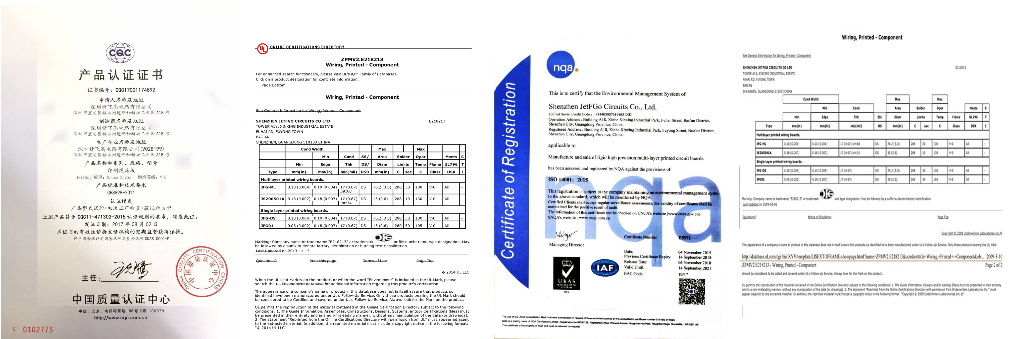
| Certificate | RoHS/ISO9001/TS16949/UL/ISO14001/ISO13485 |
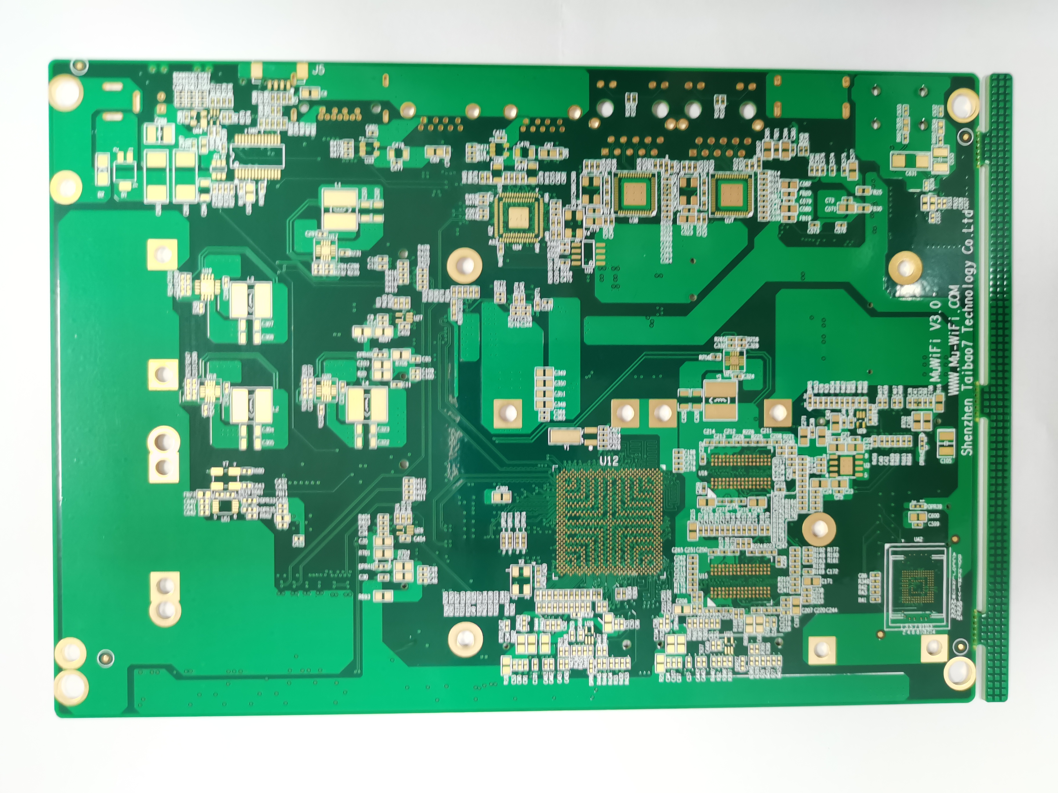
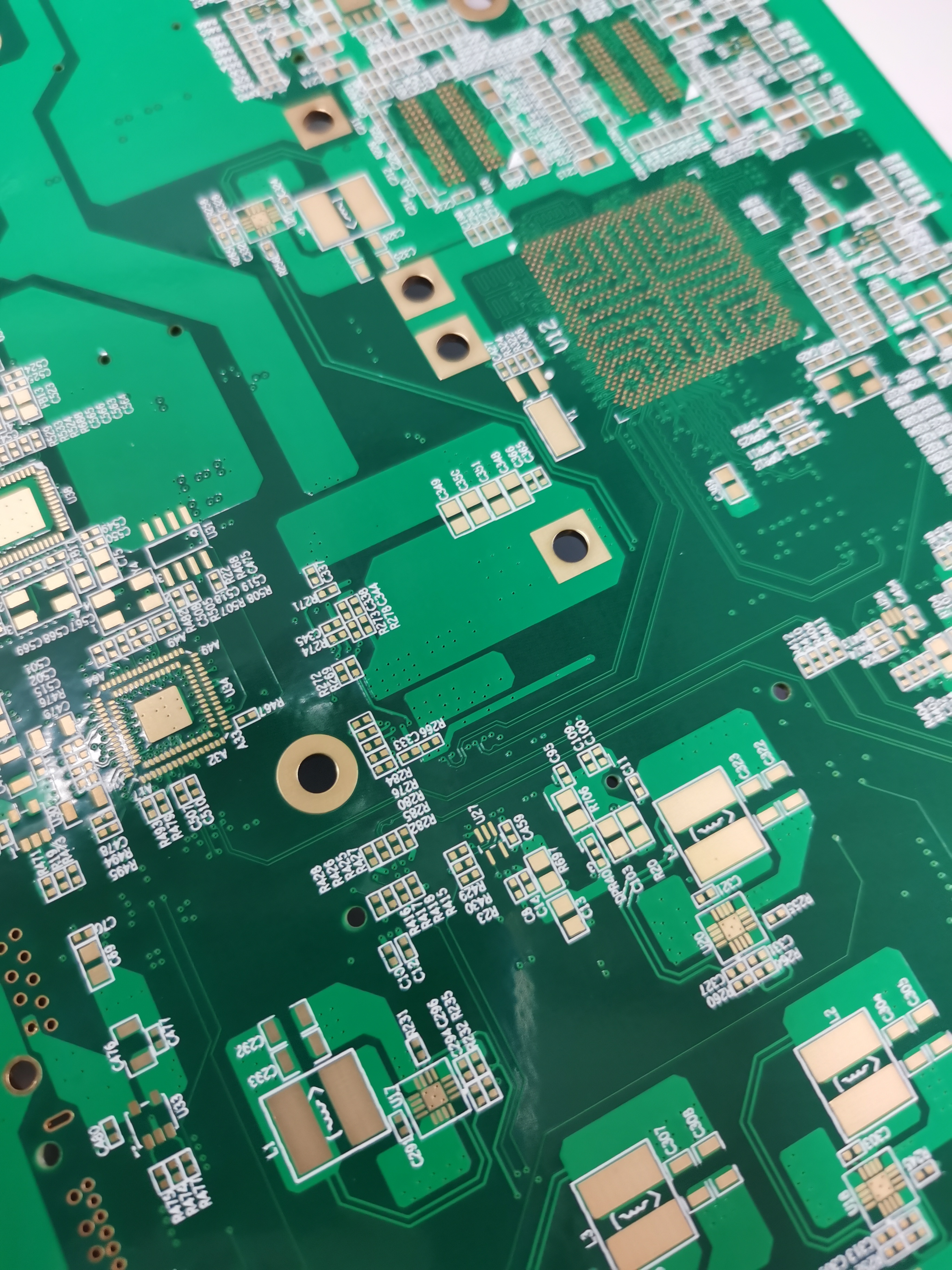
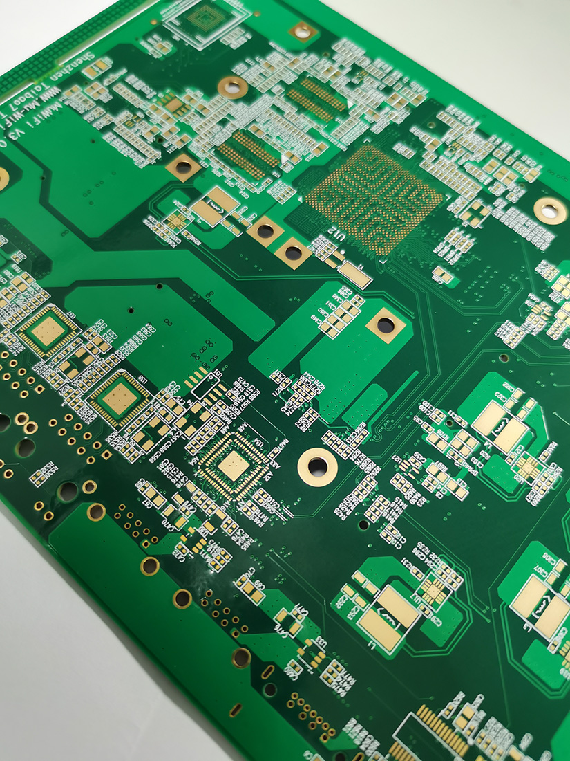
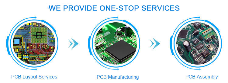
We provide the following services to our clients: Schematic Design & Board Layout, PCB & FPC Manufacturing, Metal Injection Molding, Global Supply Chain Management, and PCB & PCB Assembly Service. We deliver finished goods to you or provide drop shipping. If you require only one aspect of the above, we have the flexibility to match your needs and requirements.
We provide one-stop PCBA service, such as 0201/BGA/CCGA surface-mount (SMT), thru-hole (THT), mixed technology (SMT & thru-hole), conformal coating, potting and encapsulations, AOI/X-Ray PCBA testing, IC programming, box building service, etc.
Our PCBA solutions are used in telecommunications, automotive electronics, 3G/4G/5G products, IOT products, AI smart control products, RF, networking, security, industrial control, medical instrumentation, military products, computer peripherals and other high-tech fields. We have a great reputation from our customers around the world.