
As global hygiene mandates shift toward chemical-free, energy-efficient disinfection, ultraviolet-C (UVC) light-emitting diode (LED) technology has emerged as the definitive standard for localized pathogen inactivation.
Traditional low-pressure mercury vapor lamps are rapidly being phased out globally due to Minamata Convention restrictions, paving the way for solid-state UVC semiconductors. Operating in the germicidal wavelength band of 260nm to 280nm, UVC LEDs disrupt the cellular DNA and RNA structures of viruses, bacteria, and spores, preventing replication with log-reduction rates up to 99.999% (Log 5).
However, integrating high-power UVC LEDs into rugged, long-life industrial systems presents severe engineering challenges. Specifically, only 3% to 5% of electric energy supplied to an AlGaN (Aluminum Gallium Nitride) chip is converted into optical output; the remaining 95% is generated as heat. Solving these core thermal, electrical, and control constraints requires direct collaboration with an integrated industrial hardware and semiconductor solutions manufacturer.
To maximize external quantum efficiency (EQE), engineers must address crystal defect densities in AlGaN layers on sapphire substrates. Additionally, advanced driving circuit designs (optimized PCBs) and highly conductive thermal interfaces (water blocks and heavy copper heatsinks) are critical to keeping the junction temperature below 60°C, preserving the L90 operating lifetime exceeding 10,000 hours.
Founded & Standardizing Excellence
Modern R&D & Manufacturing Facility
Annual International Export Revenue
Global Supply Chain Partners
A leading-edge hardware, storage, and semiconductor subsystem engineering partner supporting industrial, commercial, enterprise, and consumer product lines globally.
Operating from a state-of-the-art 18,600 m² facility, Cynovex integrates R&D, production, quality control, and international sales. We offer comprehensive customization including private labeling, logo printing, packaging, firmware optimization, capacity selection, and performance tuning.
To ensure unmatched reliability, every single hardware run undergoes 100% functional testing, burn-in testing, compatibility verification, signal integrity analysis, and aging testing. A dedicated staff of 56 quality inspectors guarantees global standards compliance.
With a dedicated team of 94 engineers, we successfully designed and launched 138 new products last year. This rapid design-to-mass-production cycle allows our partners across North America, Europe, and Asia to stay ahead of market dynamics.
China's unmatched manufacturing clusters provide deep supply-chain stability, raw material access, and hardware optimization expertise.
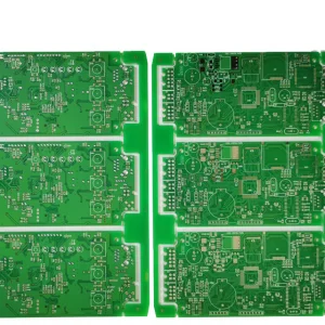
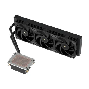
China-based production clusters permit seamless access to double-sided and multilayer printed circuit boards, high-grade copper heat sinks, and server-grade liquid water-cooling blocks. By integrating these component lines directly, manufacturers drastically lower assembly overhead and optimize thermodynamic footprints before shipping final products to global system integrators.
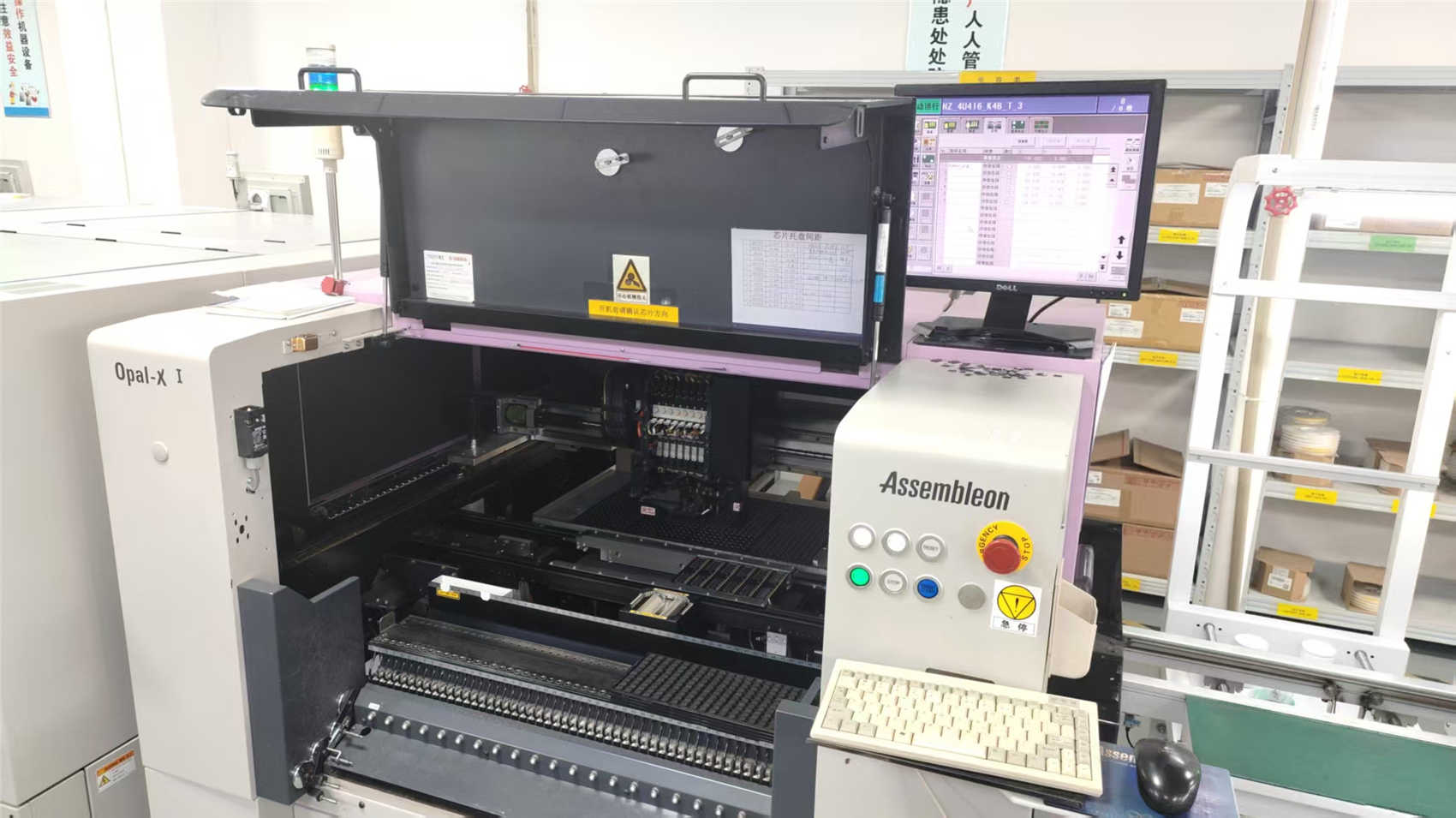
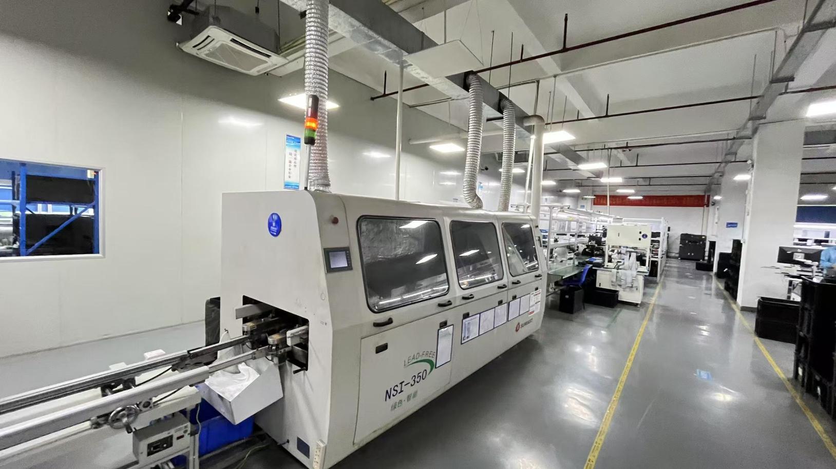
Our factories utilize high-speed Surface Mount Technology (SMT) lines capable of mounting sensitive quartz-glass lens UVC LEDs without damaging optical structures. Automated optical inspection (AOI) ensures that solder interfaces have minimal voids, achieving high heat transfer rates away from the diode junction.
Bridging the gap between raw semiconductor technology and functional, real-world deployment across municipal, commercial, and industrial facilities.
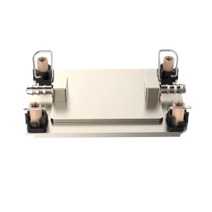
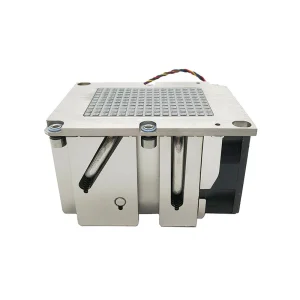
Flow-through reactor units requiring high-intensity radiation flux. Requires custom heavy-duty water cooling blocks to dissipate high-power heat generation and specialized double-sided control boards for smart monitoring.
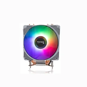
In-duct air disinfection matrices. High-flow dynamic environments need aluminum-finned heat pipe thermal designs and robust microcontrollers to withstand continuous operation and moisture.
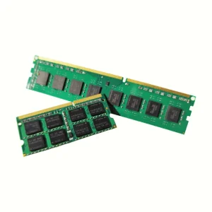
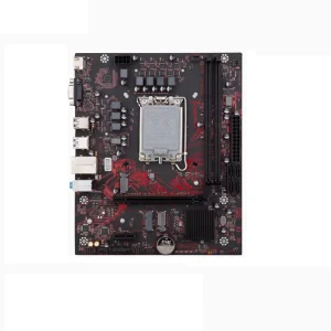
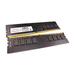
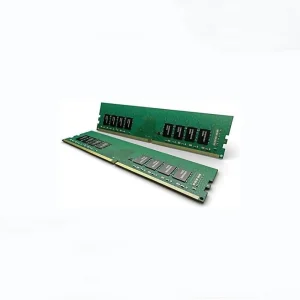
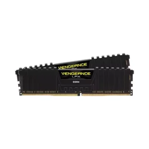
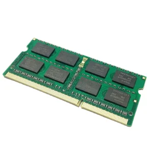
Autonomous robotics and surface scanners require embedded industrial computer motherboards, robust DDR memory kits to process local computer-vision safety tasks, and reliable high-density circuit routing.
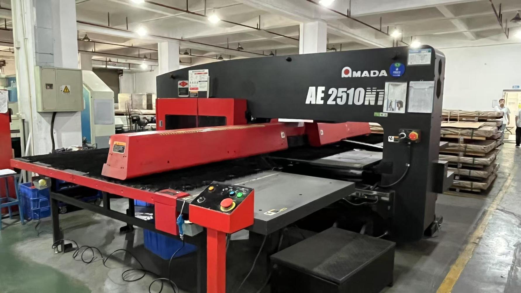
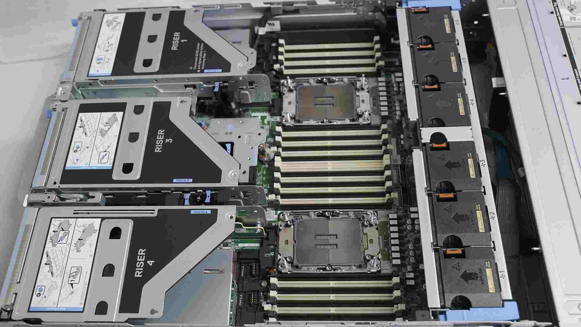
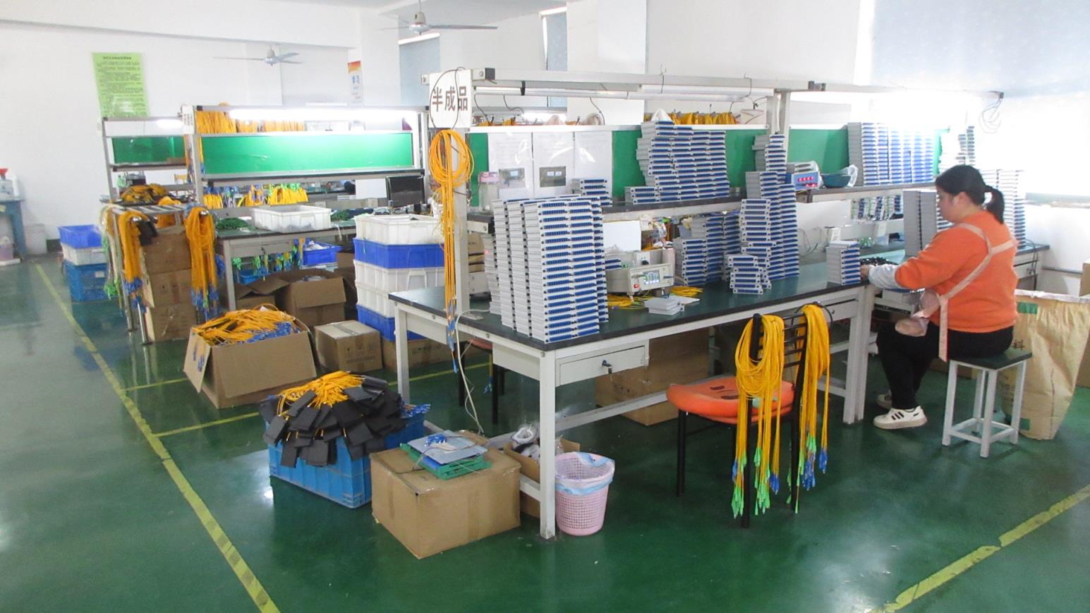
A glimpse inside our specialized laboratories, automated production floors, and testing chambers.
Essential integration insights for global procurement officers, project managers, and systems architects.
High-power UVC LEDs convert over 95% of electrical energy into thermal energy at the AlGaN chip junction rather than emitting light. If this heat is not aggressively transferred away from the chip using low-resistance copper interfaces or water-cooling blocks, the junction temperature rises rapidly. This causes a dramatic drop in optical output power, accelerates spectral shift, and can result in premature component failure.
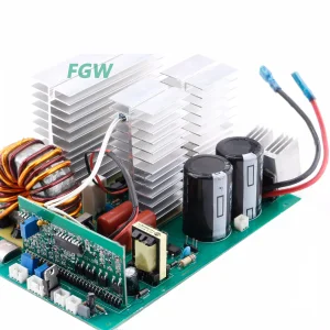
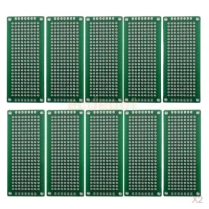
Custom double-sided or multi-layer FR4/Metal Core PCBs serve as the physical and electrical backbone for UVC arrays. They supply highly stabilized constant-current driver circuitry, which is vital because UVC diodes are sensitive to current fluctuations. Advanced driver motherboards also integrate sensors for temperature and optical intensity monitoring, ensuring safe and reliable operation.
With 94 design and R&D engineers, we manage the entire customization cycle. This starts with schematic capture and PCB layout design, moves through thermal simulation and thermal management engineering (such as copper heat sinks and liquid blocks), and finishes with custom firmware coding and testing.
Our quality control division runs a comprehensive testing regime. Every production batch is subjected to 100% functional validation, prolonged thermal burn-in, signal integrity optimization, packaging drop tests, and humidity chamber aging. This ensures all shipped hardware meets international industrial standards.
 Cynovex