Optimized layout options for advanced automated surface mount technology (SMT) operations across Swiss precision engineering lines.
Switzerland has long stood at the pinnacle of micro-manufacturing, driven by its world-renowned watchmaking heritage (the Jura Arc), cutting-edge medical device industry (Basel and Zurich), and high-reliability aerospace defense sectors. As printed circuit board (PCB) assemblies in these high-precision sectors transition rapidly to high-density layouts (HDI), the demand for ultra-precise solder paste deposition has intensified.
Laser Stencils represent the key technological bridge that turns modern sub-millimeter component designs—such as 01005 passives, ultra-fine-pitch Ball Grid Arrays (BGAs), and complex QFN packages—into physical realities. Traditional etching methods fall short of the microscopic tolerances needed for Swiss manufacturing. Today, Swiss electronics manufacturing services (EMS) rely heavily on advanced laser-cut metal stencils to ensure zero-defect assembly processes, optimizing transfer efficiency and avoiding costly paste bridges.
Aperture design is the science at the heart of modern laser stencils. For reliable solder paste release, structural design rules based on Area Ratio ($A_r$) and Aspect Ratio ($A_s$) are strictly applied. In Swiss high-reliability medical technology, where failures are not an option, stencils must maintain an Area Ratio greater than 0.66:
Using state-of-the-art fiber laser systems with a focused spot diameter down to 20µm, stencils are produced with smooth taper angles (typically 1.5° to 2°), facilitating clean solder paste exit. By matching the optimal stainless steel foil thickness (ranging from 80µm to 250µm) with advanced nano-coatings, the transfer efficiency of solder paste is enhanced, minimizing clean cycles and maximizing production speed.
Engineered to meet the exact mechanical requirements of modern Swiss Surface Mount Technology lines.
Address varying component heights on a single board layout. By using micro-welding or precision chemical milling, we create localized variations in stencil thickness, ensuring correct paste volume for both large thermal pads and fine-pitch components.
Polymeric coatings applied to the contact and aperture wall surfaces of the stencil. This technology repels solder paste, reducing under-stencil cleaning frequency by up to 70% and drastically lowering solder ball defects.
Utilizing Fine-Grain (FG) steel foils, which have a molecular grain size of only 1-2 microns. This substrate results in much smoother cut walls than standard 304/316 stainless steels, yielding superior paste release metrics.
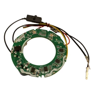
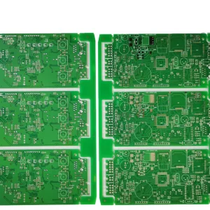
High-reliability hardware optimized via precise SMT solder paste stencil printing designs.
Managing the procurement of laser stencils within the Swiss industrial sector requires balancing rapid delivery with strict quality control. In the SMT assembly line, stencils are consumable tooling; if a stencil breaks or has layout discrepancies, the entire production line stops. Therefore, global suppliers must offer rapid turnaround times, flawless CAD-to-laser processing, and robust logistics networks to Switzerland (Zurich Airport ZRH, Geneva Airport GVA, and key rail/road corridors).
Swiss operations are bound by European-aligned environmental mandates (RoHS, REACH, and WEEE). The selection of stencil cleaning agents must conform to local VOC limits (Swiss Volatile Organic Compounds incentive tax). Consequently, stencils must possess high chemical resistance to eco-friendly, water-based cleaning agents. Furthermore, standard framed stencils generate waste; hence, there is a distinct transition toward space-saving, reusable frame systems like VectorGuard, ZelFlex, or Alpha Tetra. These systems allow Swiss manufacturers to ship or store only the thin stainless steel foil, reducing freight costs and minimizing physical storage space inside cleanroom assembly areas.
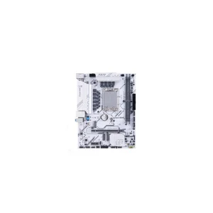
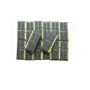
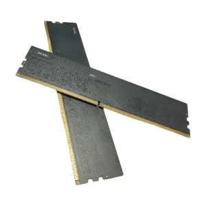
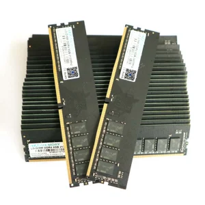
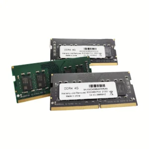
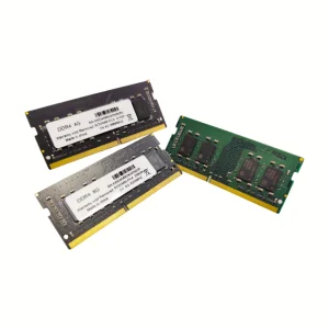
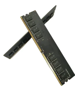
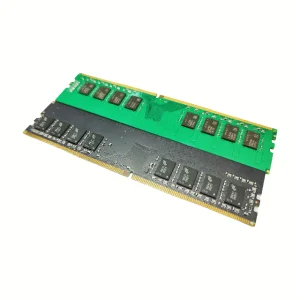
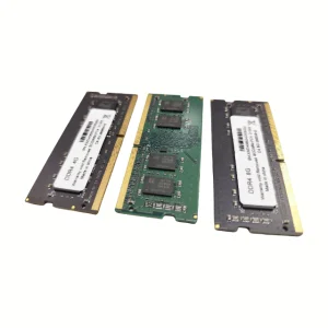
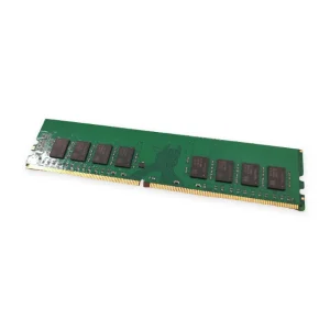
As a global leader in high-reliability components, Cynovex Semiconductor Co., Ltd. applies its extensive SMT assembly expertise directly to its manufacturing support paradigms. Established in 2016, our facility spans 18,600 m² and operates with 94 dedicated R&D engineers. We understand the critical nature of stencil aperture design because we run high-speed SMT lines ourselves to manufacture advanced memory solutions, including DDR5 and DDR4 modules.
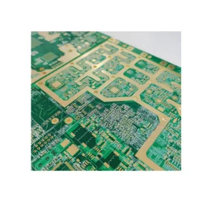
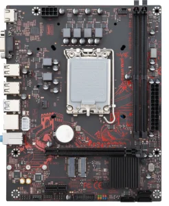
In high-speed DDR5 module assembly (5600MHz - 6000MHz), signal integrity is paramount. Solder joint height variations, caused by poor stencil aperture uniformity, can introduce parasitic capacitance, leading to data transmission errors. Cynovex uses electro-polished laser stencils internally to assemble DDR5 memory modules and high-frequency PCBs, achieving ultra-flat solder deposits on BGAs. We leverage this direct manufacturing experience to assist Swiss clients with stencils designed specifically for challenging high-speed memory and RF layouts.
Our operations integrate strict QA controls and robust engineering resources to deliver reliable micro-components globally.
Our quality assurance program is backed by 100% functional testing, signal integrity evaluation, and dynamic burn-in chambers. Every batch of SMT components and metal stencils is validated against IPC-A-610 standards.
As the microelectronics industry targets sub-micron nodes, several technological shifts are transforming laser stencil design and application across Europe:
Swiss engineers must partner with agile manufacturers who quickly adapt to these technical advances, ensuring early access to prototype designs and short production cycles.
Technical clarifications on laser stencil design, materials, and Swiss market procurement logistics.
Fine-Grain (FG) steel contains alloying elements that produce a tight, uniform molecular structure. When cut with fiber lasers, the edge roughness is significantly lower compared to standard SUS304 steel. This reduction in micro-fractures on the aperture walls facilitates complete solder paste release, which is critical for ultra-small component prints like 01005 passives.
We calculate thickness variations based on the component density and layout of adjacent pads. If a high-power power-transistor pad requires a large volume of paste (requiring 150µm thickness) but sits next to a 0.4mm pitch BGA (requiring 100µm thickness), we design a step-down pocket. The slope angle must be managed (usually 1:36 or 1:40 ratio) so the SMT squeegee blade can conform smoothly without skipping.
Standard factory-applied nano-coatings are baked on at high temperatures for long durability. While there are wipe-on room-temperature cure aftermarket nano-coatings, their mechanical wear resistance is significantly lower. We recommend using premium, factory-bonded nano-coatings for high-volume SMT lines in Swiss manufacturing facilities.
All exports are processed through reliable air-freight networks with full customs documentation, meeting Swiss Federal Customs Administration guidelines. We handle standard HS tariff classification, RoHS/REACH compliance documentation, and coordinate with local Swiss custom brokers to ensure swift, uninterrupted delivery to your manufacturing facility.
Founded in 2016, Cynovex Semiconductor Co., Ltd. is a professional manufacturer specializing in high-performance memory and advanced SMT solutions for industrial, commercial, and enterprise applications. Operating from a modern manufacturing facility covering 18,600 m², we integrate R&D, production, quality control, and international sales under one roof. Supported by an experienced engineering team and advanced manufacturing processes, we deliver high-reliability products that meet the strict requirements of global high-tech markets.
Our annual export revenue exceeds USD 28 million, supported by 8 years of international export experience and 10 years of industry expertise. Every product undergoes rigorous quality assurance using 100% functional testing, burn-in testing, compatibility testing, signal integrity testing, and aging tests. A dedicated team of 56 quality inspectors ensures that every shipment meets strict international quality standards.
As an experienced OEM & ODM manufacturer, Cynovex serves customers across North America, Europe, Southeast Asia, the Middle East, South America, and Oceania. We maintain long-term partnerships with more than 1,150 supply chain partners, enabling stable material sourcing and efficient production.
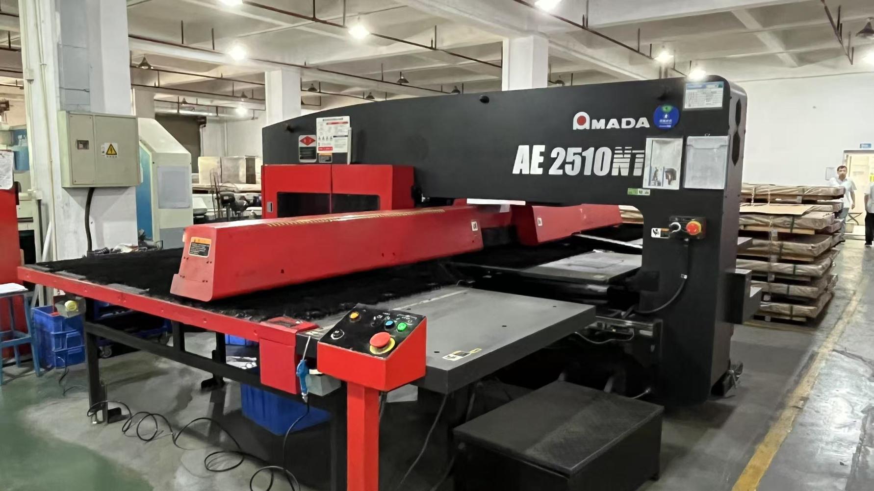
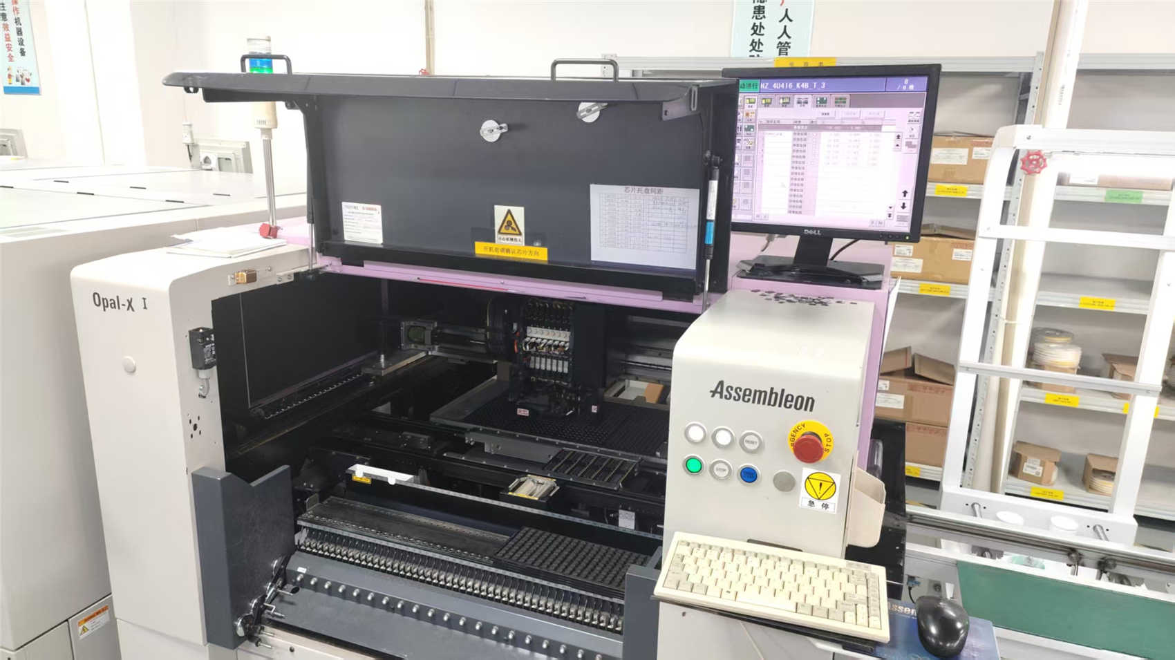
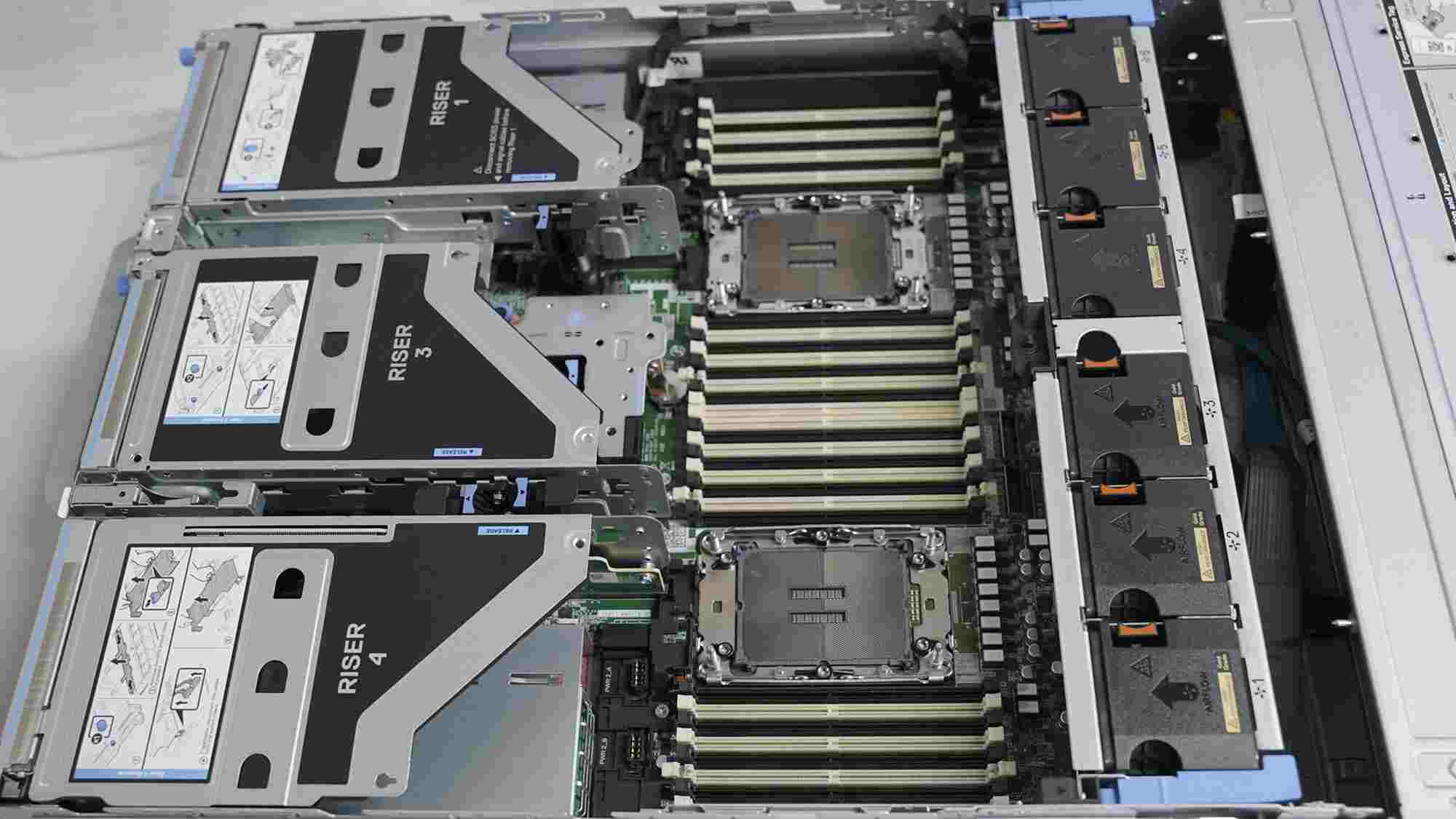
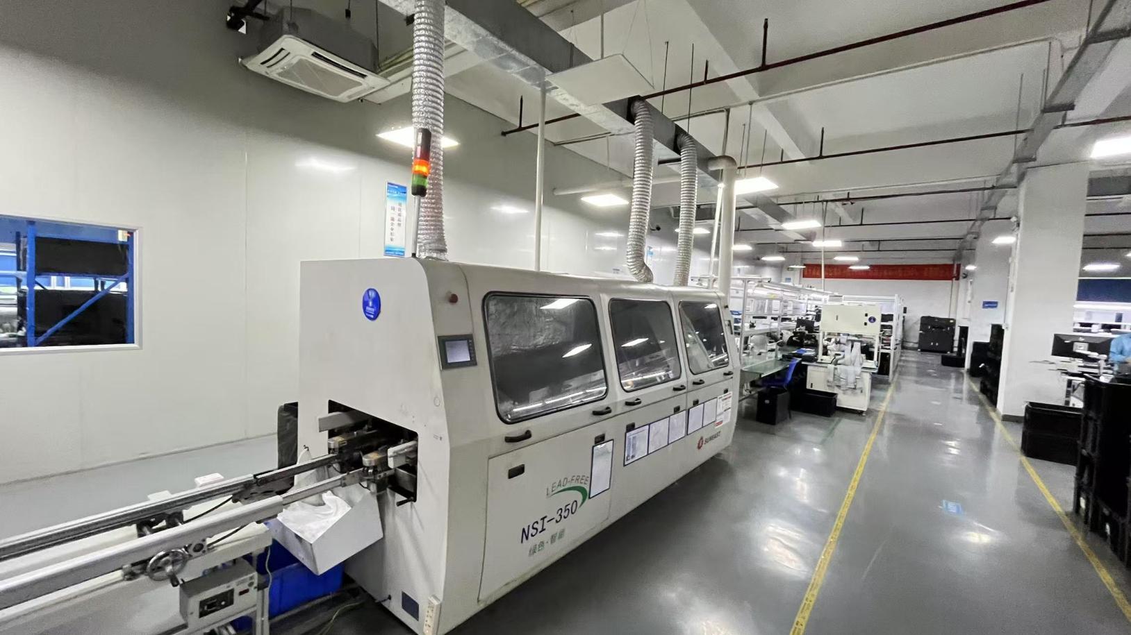
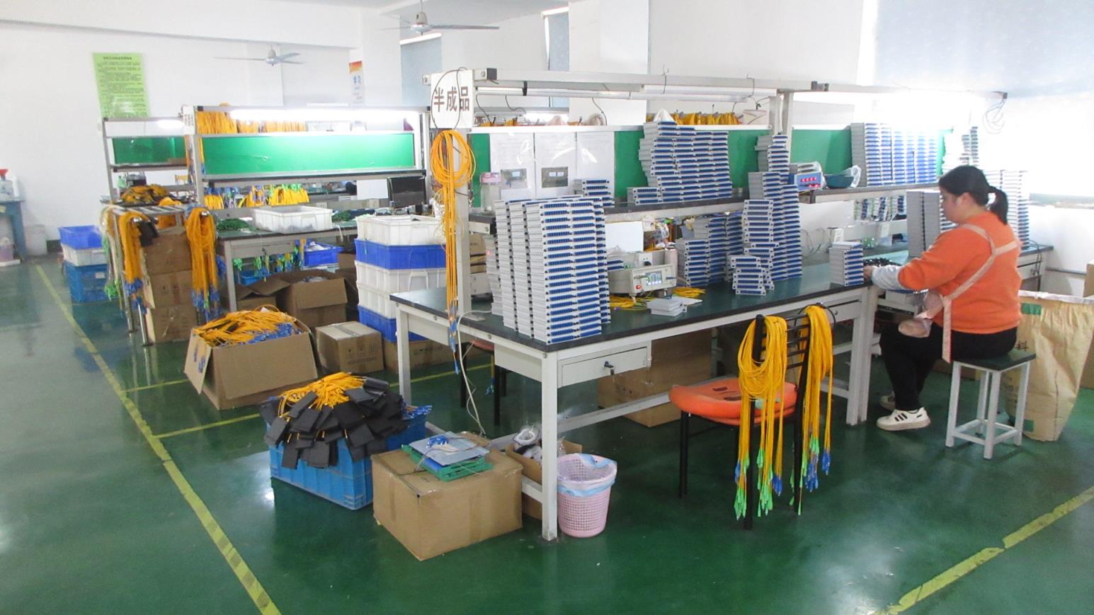
Ensure microelectronic stability and thermal efficiency with SMT-certified memory modules, controllers, and heat dissipation units.
 Cynovex