Cynovex
1 / 5
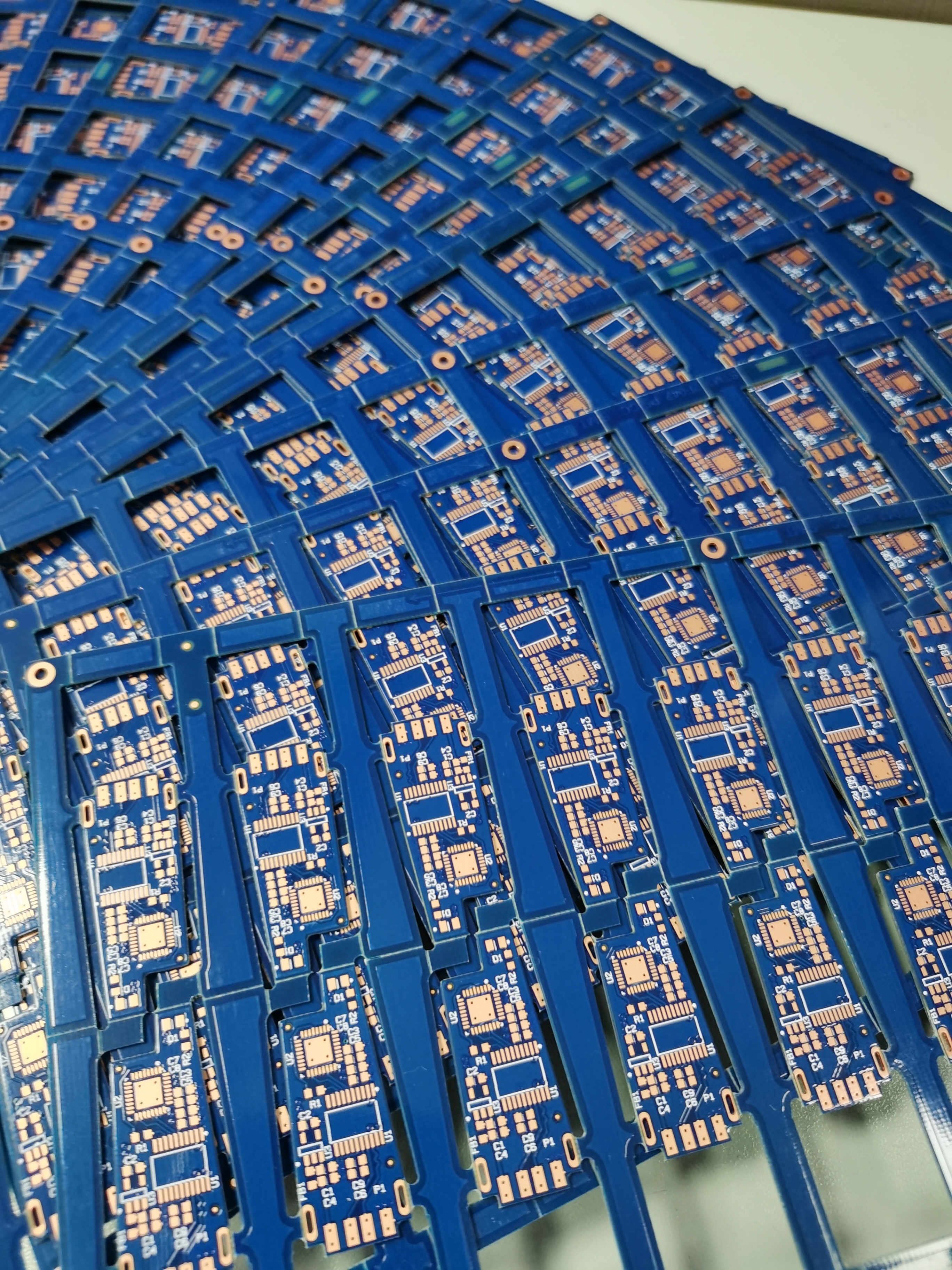
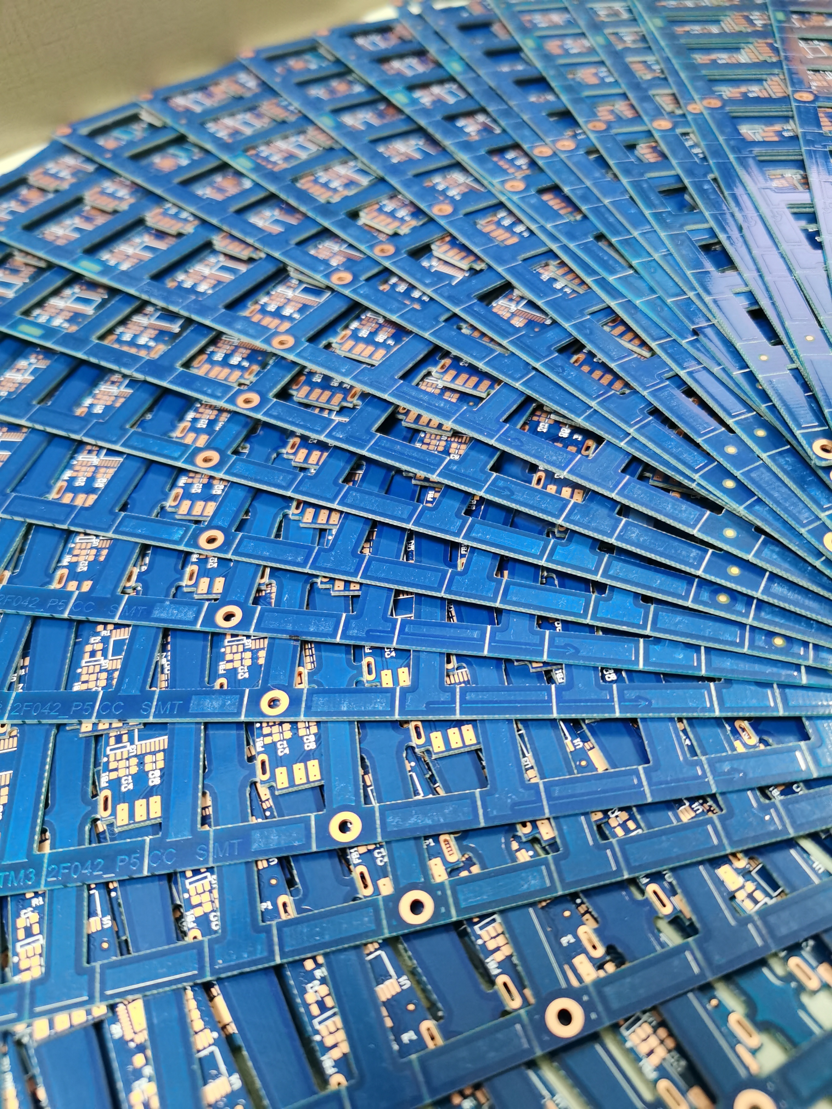
| Items | Capacity |
|---|---|
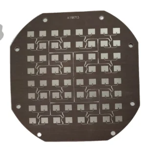
| 1. Material | FR4, (High Tg, General Tg, Middle Tg), Lead-Free Solder Sheet, Halogen Free, Ceramic Filling, Teflon, PI, BT, PPO, PPE etc. |
| 2. Board thickness | Mass production: 394mil(10mm) Samples: 17.5mm |
| 3. Surface finish | HASL, Immersion Gold, Immersion Tin, OSP, ENIG + OSP, Immersion Silver, ENEPIG, Gold Finger |
| 4. PCB Max panel size | 1150mm × 560mm |
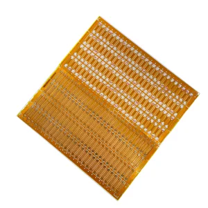
| 5. Layer | Mass production: 2~58 layers / Pilot run: 64 layers, Flexible PCB: 1-12 Layers |
| 6. Min hole size | Mechanical drill: 8mil(0.2mm) Laser drill: 3mil(0.075mm) |
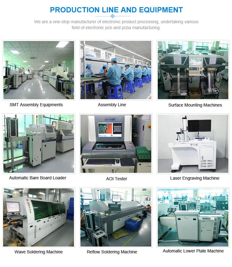
| 7. PCBA QC | X-ray, AOI Test, Functional Test |
| 8. Special Process | Buried Hole, Blind Hole, Embedded Resistance, Embedded Capacity, Hybrid, Back drilling, and Resistance control. |
| 9. Our service | PCB, Turnkey PCBA, PCB Clone, Housing, PCB Assembly, Component sourcing, 1 to 64 layers One stop services. |
| 10. SMT Capacity | 700 Million Points/Day |
| 11. DIP Capacity | 0.5 Million Points/Day |
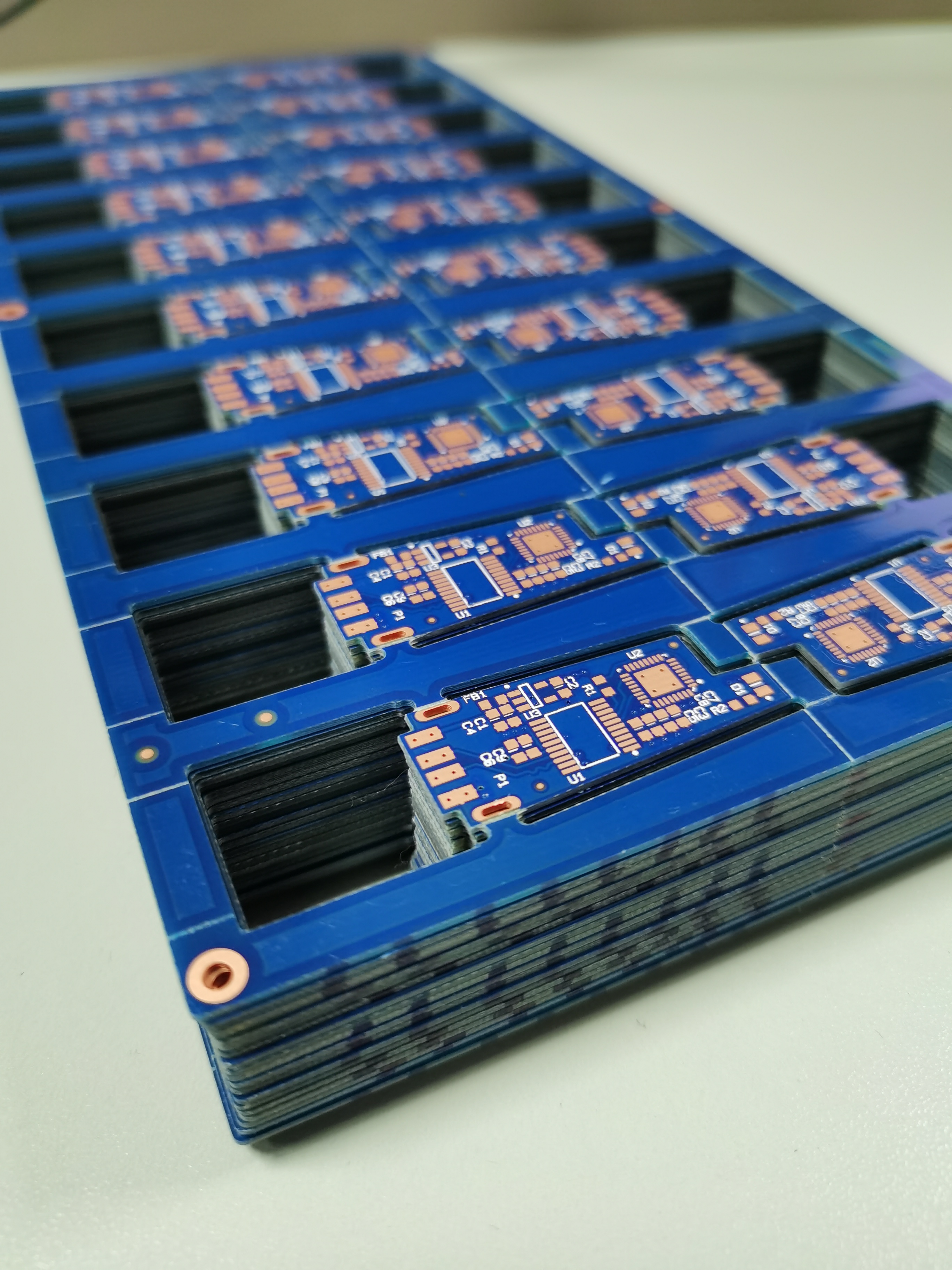
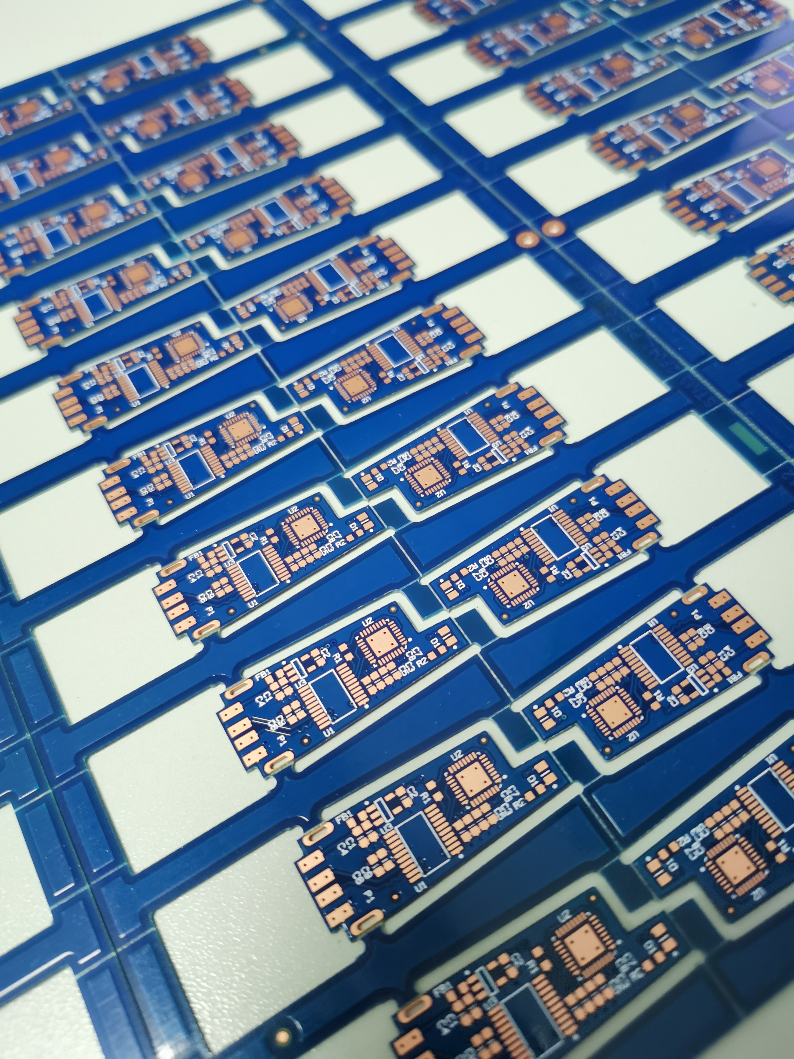
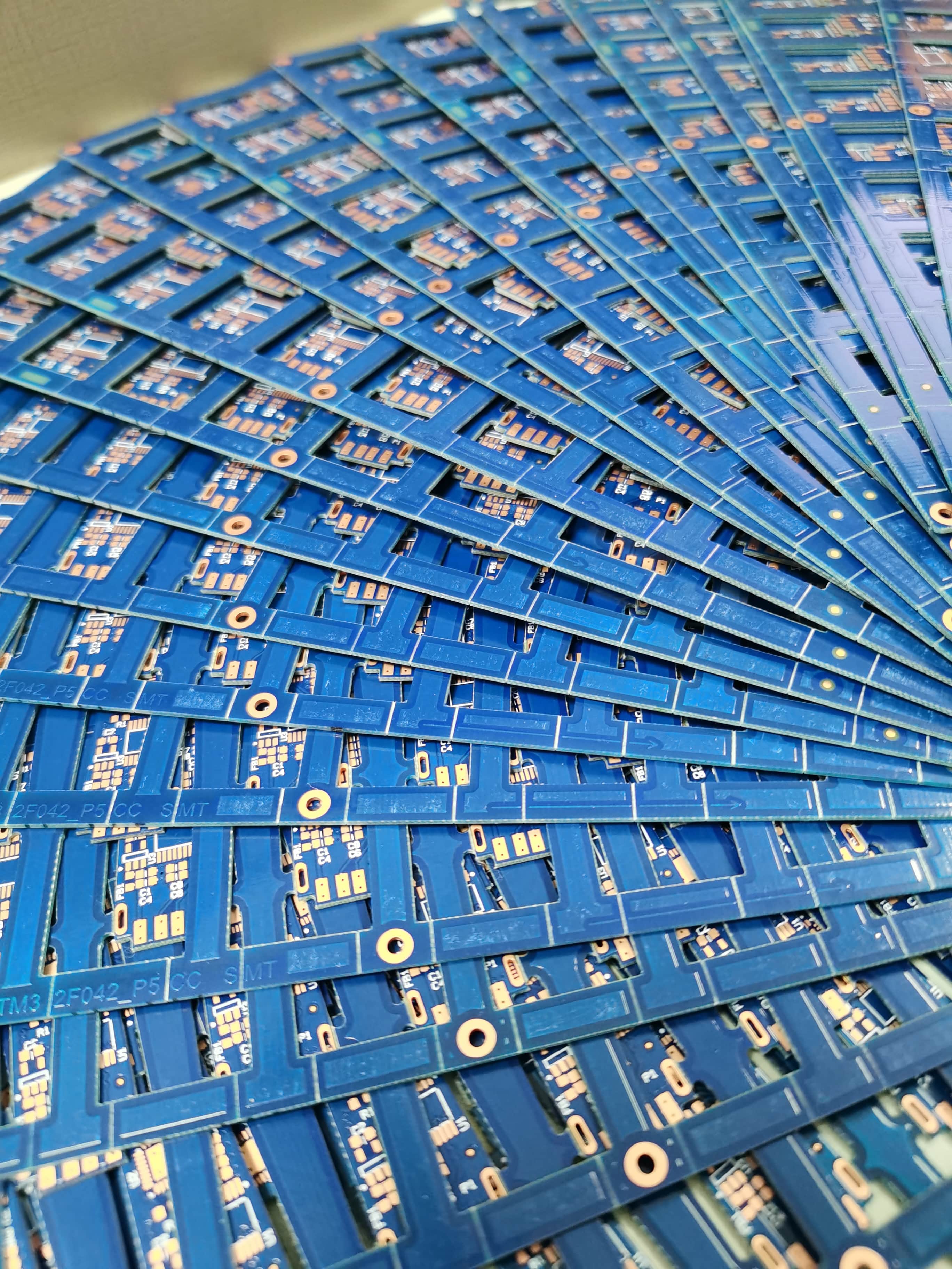
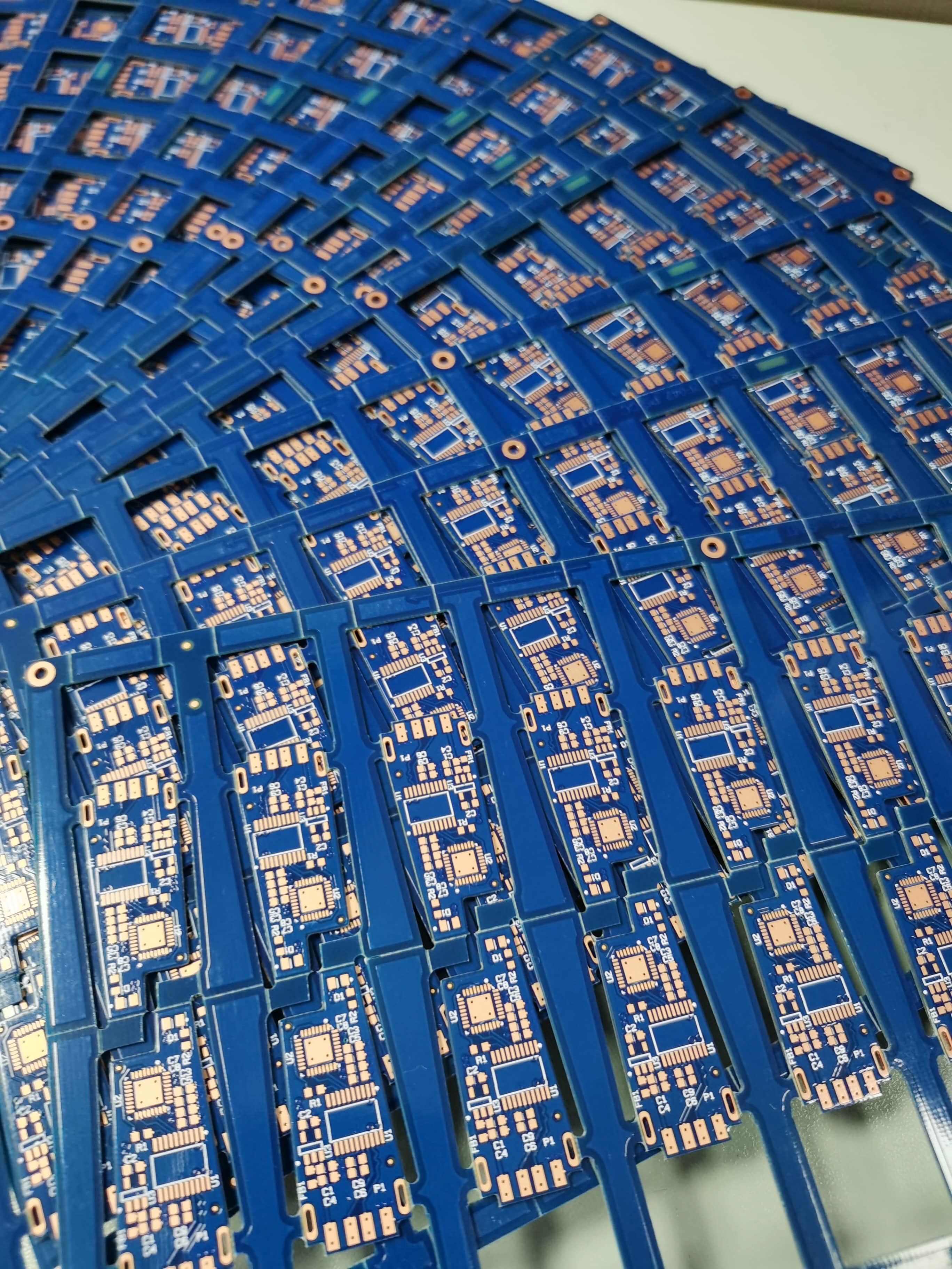
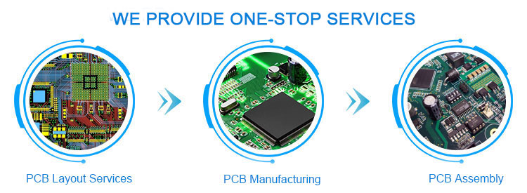
Comprehensive Solutions: We provide the following services to our clients: Schematic Design & Board Layout, PCB & FPC Manufacturing, Metal Injection Molding, Global Supply Chain Management, PCB & PCB Assembly Service. We deliver finished goods or provide drop shipping options tailored to your requirements.
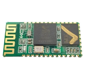
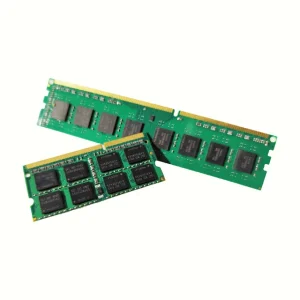
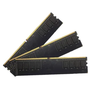
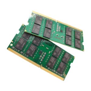
One-Stop PCBA: We provide services such as 0201/BGA/CCGA surface-mount (SMT), thru-hole (THT), mixed technology, conformal coating, potting and encapsulations, AOI/X-Ray testing, IC programming, and box building services.
Wide Application: Our products are used in telecommunications, automotive electronics, 3G/4G/5G, IOT, AI smart control, RF, networking, security, industrial control, medical instrumentation, and other high-tech fields.