Industrial-Grade Memory Modules and Circuit Assemblies Optimized for High-Reliability Nano-Coated Implementations
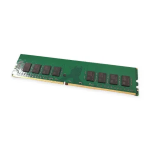
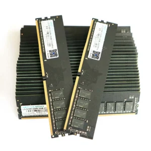
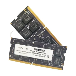
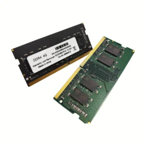
Redefining Environmental Resistance and Lifespan Extension for Microelectronics
Utilizing Chemical Vapor Deposition (CVD) and Plasma-Enhanced Chemical Vapor Deposition (PECVD), we deposit protective fluoropolymer and Parylene matrices at thicknesses ranging from 10nm to 50μm. This guarantees comprehensive pinhole-free coverage without compromising contact resistance, heat dissipation pathways, or signal integrity on fine-pitch components.
By tailoring surface energy properties, our nano coatings achieve contact angles exceeding 115° for water and 85° for organic solvents. Liquid runs off immediately, preventing moisture retention, surface track path formation, dendritic growth, and electrochemical migration on high-density circuits.
Engineered to resist corrosive environments, acidic and alkaline cleanings, and high salt-spray conditions, our coatings maintain structural integrity from -65°C to 150°C without degradation, outgassing, or cracking under thermal cycling conditions.
In modern microelectronics—where trace widths are down to microns—humidity, ambient moisture, sulfur, gaseous pollutants, and microscopic dust are primary failure vectors. Traditional silicone, acrylic, or polyurethane conformal coatings add significant thermal resistance, increase weight, and change high-frequency electrical characteristics (permittivity).
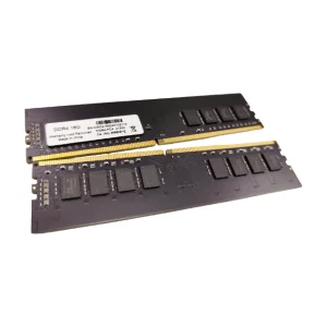
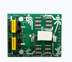
Our custom OEM Nano Coatings deposit ultra-thin, highly uniform polymeric matrices. These materials wrap around complex geometric configurations, including solder joints under BGA components, the pins of fine-pitch DDR memory chips, and high-density multi-layer PCBs. This level of protection prevents mechanical failures without trapping heat or shifting critical impedence balances.
Uncovering the Growth and Crucial Mandate of Nano Conformal Protection in Global Supply Chains
The global electronic protection market is shifting rapidly from mechanical containment (IP-rated enclosures) to component-level resilience. This transformation is driven by several key factors:
| Coating Technology Class | Typical Thickness Profile | Dielectric Strength (V/μm) | Primary Industrial Use Case | Thermal Conductivity (W/m·K) |
|---|---|---|---|---|
| Parylene C/N CVD | 1.0 μm - 15 μm | > 200 | Aerospace, Military Avionics, Medical Devices | 0.08 - 0.12 |
| Plasma Fluoropolymer | 50 nm - 500 nm | N/A (Ultra-thin barrier) | Consumer Electronics, Handhelds, PCBs | 0.15 - 0.22 |
| Atomic Layer Deposition (ALD) | 5 nm - 50 nm | > 400 | MEMS, Semiconductor Die Passivation | 1.1 - 2.5 |
| Acrylic / PU (Traditional) | 25 μm - 125 μm | 30 - 60 | Heavy Industrial Power Controls | 0.10 - 0.18 |
How Cynovex Customized Protection Solves Environmental Threats Across Global Climatic Regions
Climatic Stress: Average relative humidity above 85% and high ambient temperatures accelerate electrochemical migration and corrosion.
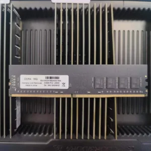
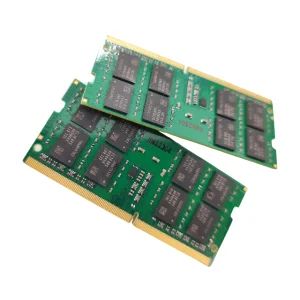
Cynovex Solution: Ultra-thin hydrophobic plasma coatings applied to our industrial DDR4 Laptop and Desktop modules. This setup prevents condensation-induced leakage currents and dendritic growth on components, securing continuous operation in tropical factories and smart cities.
Climatic Stress: Extreme temperatures, thermal shock (day-to-night delta >30°C), and high penetration of fine abrasive dust particles.
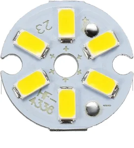
Cynovex Solution: Dual-layer hybrid coating. First, a hard SiO2-like barrier, followed by a hydrophobic topcoat. This approach resists sand erosion on outdoor inverter boards, telecom switches, and LED drive circuits, keeping control systems dust-tight and thermally stable.
Climatic Stress: High salinity, chlorine-laden marine air, and continuous exposure to salt water spray.
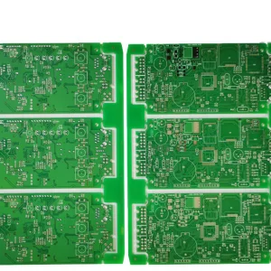
Cynovex Solution: Parylene-C CVD coatings applied directly to high-frequency aluminum substrate PCBs and water-cooled server heat sinks. The result is a robust barrier that blocks chloride ions and guards against galvanic corrosion.
Cynovex Semiconductor Co., Ltd. - Integrating Quality Assurance, OEM Customization, and Global Logistics
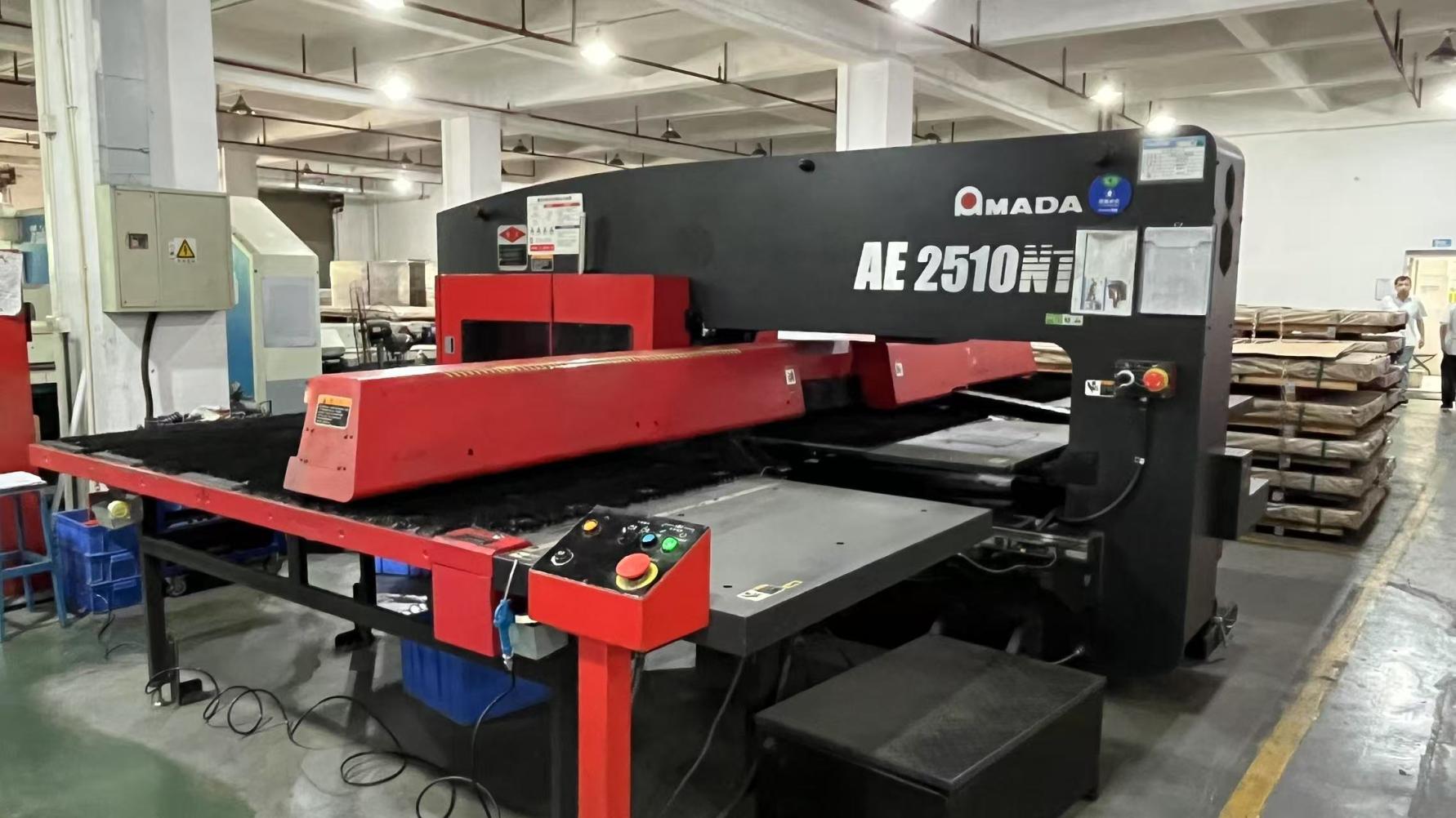
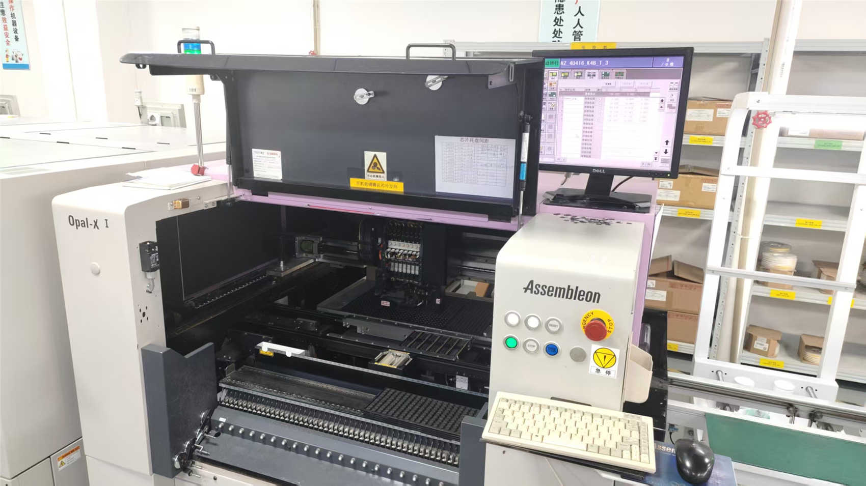
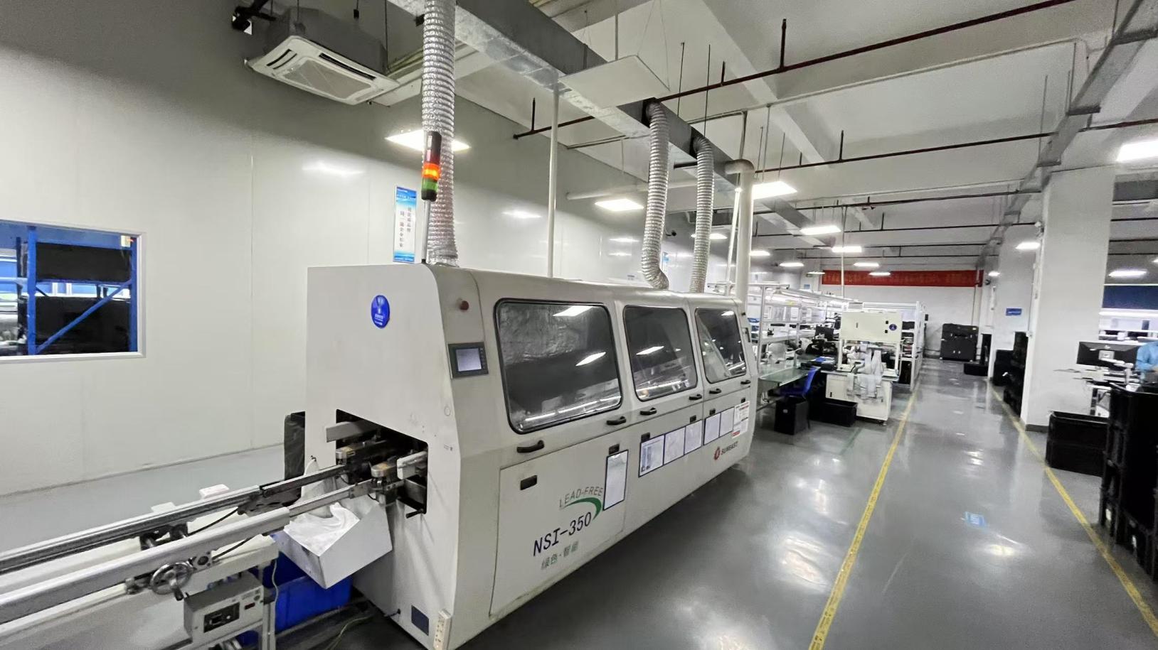
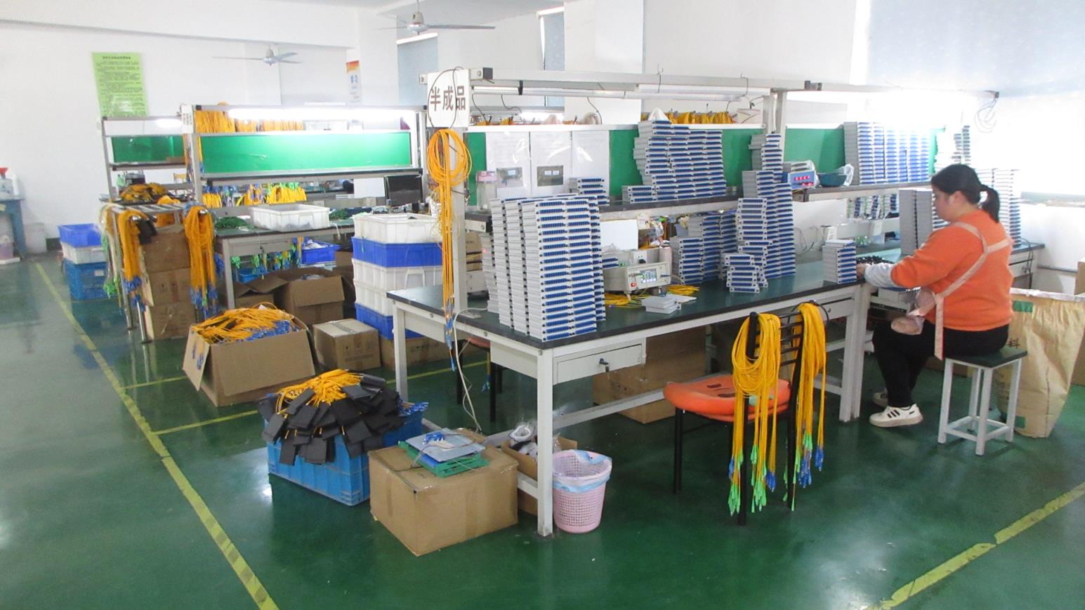
Founded in 2016, Cynovex Semiconductor Co., Ltd. is a professional manufacturer specializing in high-performance memory and hardware solutions for industrial, commercial, enterprise, and consumer applications. Operating from a modern manufacturing facility covering 18,600 m², we integrate R&D, advanced production, automated nano coating lines, quality control, and international sales under one roof.
Our annual export revenue exceeds USD 28 million, supported by 8 years of international export experience and 10 years of industry expertise. We maintain long-term partnerships with more than 1,150 supply chain partners, enabling stable material sourcing, consistent quality, and efficient production turnaround times.
To ensure outstanding reliability, every memory module, customized PCB, and coated board undergoes rigorous validation protocols within our facility. This includes:
Adapting to Regulatory Demands and Advanced Packaging Shifts in Electronics Protection
Global regulatory developments (like REACH, TSCA, and upcoming PFAS restrictions) are driving a transition away from traditional fluoropolymer matrices. Cynovex's R&D team is actively engineering next-generation, eco-compliant hydrocarbon-based and siloxane-based molecular coatings. These materials offer the same water and chemical resistance without utilizing bio-accumulative fluorinated agents.
Micro-cracking from thermal stress and physical impact can compromise thin coatings. The future of conformal protection lies in micro-encapsulated self-healing polymer matrices. When a micro-crack develops, the encapsulated agents rupture and polymerize, sealing the breach immediately and maintaining the dielectric barrier in critical field conditions.
Traditional thick coatings act as thermal insulators. By blending high-thermal-conductivity ceramic nanowires (such as AlN or BN) into the liquid nano-suspension before chemical deposition, we create high-dielectric barrier layers that also function as thermal interface paths. This enhancement improves thermal performance on components like server RAM chips and high-power LED arrays.
Global Quality and Compliance Standards for Complex OEM Projects
We work closely with global system integrators and distributors to ensure all raw materials, manufacturing practices, and coated assemblies comply with local regulatory frameworks:
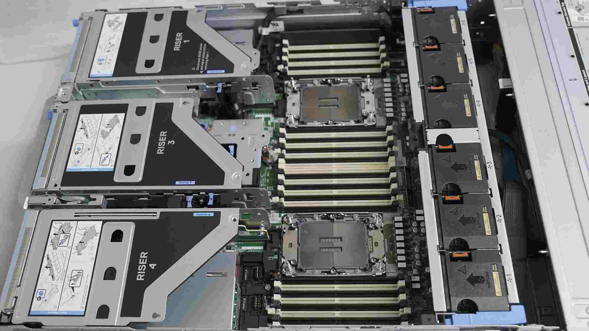
Inside our 18,600 m² Facility: High-Speed SMT Lines, Automated Nano-Coating Chambers, and Advanced QA Labs
Answers to Key Technical and Process Questions for Engineers and Procurement Managers
Premium Circuit Boards, Server Coolers, and High-Speed Components for Coated System Implementations
 Cynovex