Explore our leading-edge assemblies engineered to perform reliably in server environments, power systems, and high-frequency arrays.
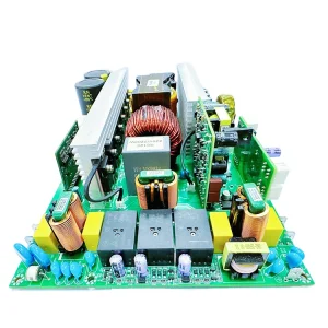
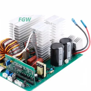
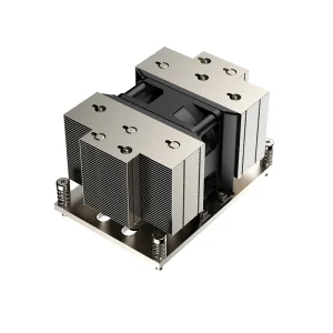
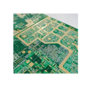
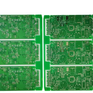
Thick copper circuit boards, universally classified in high-reliability fields as Heavy Copper PCBs, feature copper weights starting at 3 ounces per square foot (approx. 105 µm) and scaling up to 20 ounces or more. Standard boards typically operate on 1 oz (35 µm) copper lines, which fail immediately under high-voltage configurations.
By employing specialized chemical electroplating and photolithography techniques, heavy copper paths enable the PCB to become more than an interconnection highway. It transforms the board itself into a structural heat sink and high-amperage power distribution matrix. The increased trace thickness ensures the board handles thermal stresses, high ambient currents, and mechanical shocks simultaneously.
For aerospace systems, solar photovoltaic arrays, and high-load servers, incorporating thick copper layers eliminates the need for bulky external bus bars, reduces the layout area, and lowers overall assembly weight while drastically increasing mechanical reliability.
Standard trace dimensions cannot sustain excessive power losses, leading to severe thermal expansion and delamination. Heavy copper optimizes current flows, delivering key engineering advantages:
Our OEM/ODM capability allows us to customize physical layouts based on complex electrical requirements. Review our structural limits below.
| Technical Parameter | Standard Range | Advanced Heavy Copper Capabilities | Design Implications |
|---|---|---|---|
| Copper Layer Weight | 1 oz to 2 oz (35 µm - 70 µm) | 3 oz to 20 oz (105 µm - 700 µm) | Enables high-amperage handling without excess temperature rise. |
| Substrate Base Material | Standard FR-4 (Tg 130) | High-Tg FR-4 (Shengyi TG170), Rogers 4000 series mixed pressure | Withstands extreme thermal loading and high-frequency signals. |
| Minimum Trace / Spacing | 3 mils / 3 mils | 10 mils / 12 mils (depends on copper weight) | Prevents electrical bridging during micro-etching stages. |
| Maximum Layer Count | Double-sided (2 Layers) | Up to 16 layers (Mixed hybrid multilayers) | Combines high-density logic layers with high-power heavy copper traces. |
| Surface Finish Options | HASL / HASL Lead-Free | ENIG, OSP, Hard Gold, Immersion Silver | Ensures strong solder connections and prevents copper oxidation. |
Integrating state-of-the-art semiconductor engineering with massive high-power hardware supply chains.
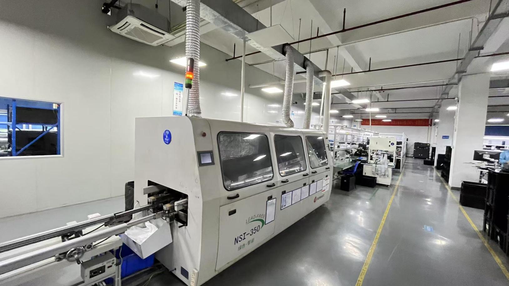
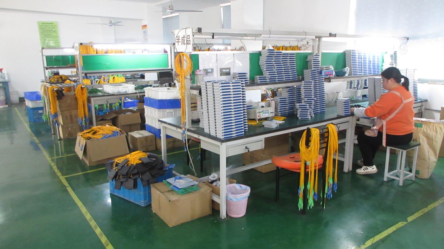
Founded in 2016, Cynovex Semiconductor Co., Ltd. is a professional manufacturer specializing in high-performance computing components and heavy-duty PCB design, including advanced memory solutions, high-current thick copper circuit boards, and industrial thermal management assemblies. Operating from a modern manufacturing facility covering 18,600 m², the company integrates R&D, production, quality control, and international sales under one roof. Supported by an experienced engineering team and advanced manufacturing processes, Cynovex provides stable, high-speed memory products and robust circuit solutions with consistent performance.
Our annual export revenue exceeds USD 28 million, supported by 8 years of international export experience and 10 years of industry expertise. Every product undergoes rigorous quality assurance using 100% functional testing, burn-in testing, compatibility testing, signal integrity testing, and aging tests. A dedicated team of 56 quality inspectors ensures that every shipment meets strict international quality standards. As an experienced OEM & ODM manufacturer, Cynovex serves customers across North America, Europe, Southeast Asia, the Middle East, South America, and Oceania. We maintain long-term partnerships with more than 1,150 supply chain partners, enabling stable material sourcing and efficient production.
Driven by quality, innovation, and customer satisfaction, Cynovex is committed to becoming a trusted global partner for reliable thick copper circuit boards, industrial control elements, high-frequency structures, and customized memory solutions.
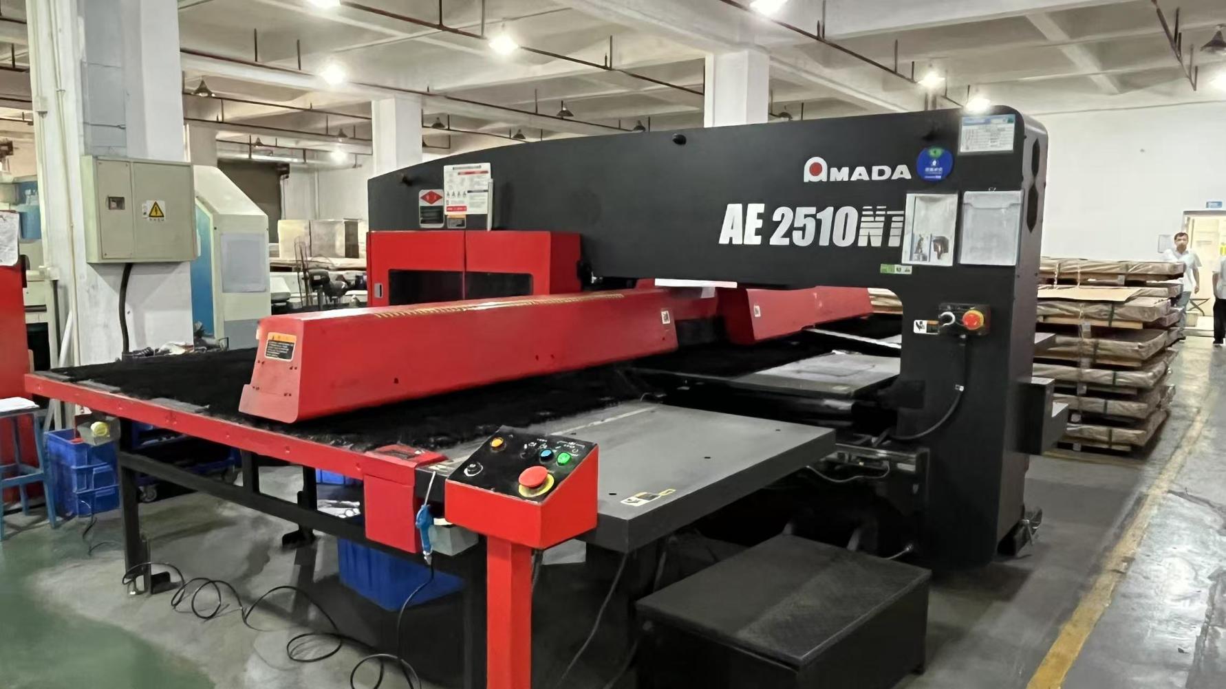
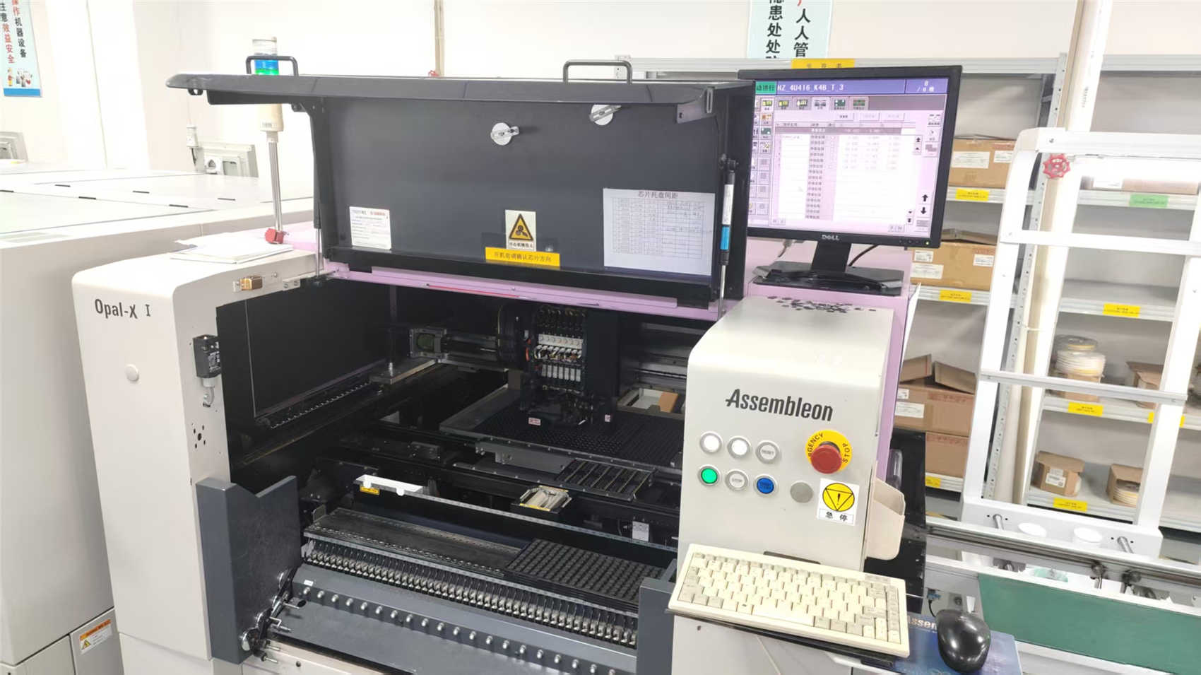
Navigating global regulatory landscapes requires rigorous compliance. We offer localized support to match complex compliance regulations including IPC-A-600 Class 3, UL 796 for thick copper safety limits, RoHS Directive 2011/65/EU, and REACH registrations. Localized warehousing and localized technical engineers in North America and Western Europe resolve integration hurdles quickly, minimizing risk.
By leveraging China's robust industrial copper ecosystem, Cynovex accesses raw electrolytic copper foils and high-performance resin sheets directly. This guarantees a steady raw material chain, shields global buyers from volatile price changes, and shortens prototype turnaround cycles. Integrated copper electroplating lines inside our factory keep costs low and output volume high.
Hardware procurement divisions demand speed, performance, and flexibility. Through our OEM/ODM workflow, we handle small-batch high-mix engineering requests as well as large mass production runs. We facilitate fast transport through major shipping terminals, offering seamless customs clearances, complete component trace audits, and reliable DDP delivery options.
Where heavy copper PCBs are driving innovation in modern electrical systems.
Modern commercial PV inverters convert vast amounts of solar power into usable grid AC electricity. This demands extreme current resilience. Our customized photovoltaic inverter PCB assemblies feature heavy copper cores (up to 8oz) that manage dynamic high-power cycles and high heat loads under harsh desert or rooftop installations.
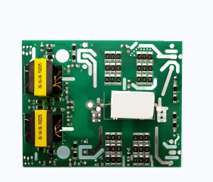
Industrial machinery like the ZX7 inverter welding motherboard utilizes heavy copper circuitry to withstand high continuous current loops. Heavy trace lines avoid thermal hotspots, keeping internal components working reliably during high-duty welding operations.
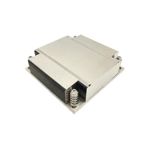
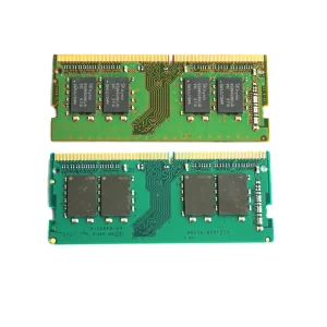
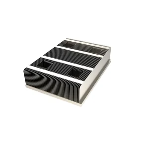
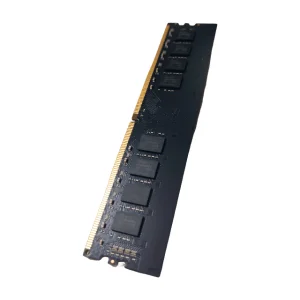
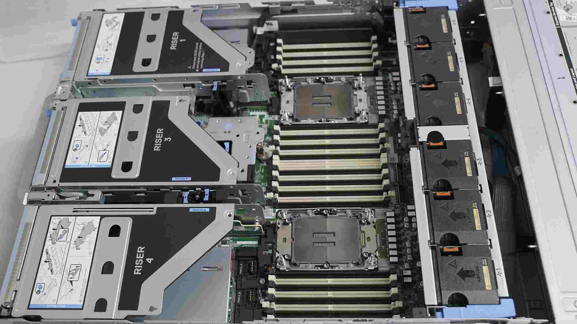
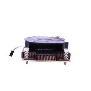
High-density data centers need both advanced CPU power delivery and excellent thermal cooling. By combining heavy copper layers with top-tier heat sinks, like the LGA4677/SP3 copper coolers and DDR5 memory modules, we deliver complete system stability for deep learning configurations.
Answering the most critical engineering and supply questions about thick copper PCB design.
Browse our enterprise-grade memory systems, server cooling components, and robust industrial baseboards.
 Cynovex